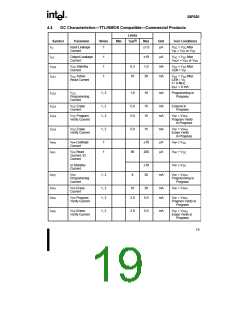
28F020
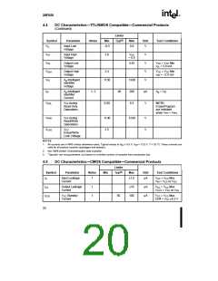
4.4
E
DC Characteristics—TTL/NMOS Compatible—Commercial Products
(Continued)
Limits
Typ(3)
Symbol
Parameter
Notes
Min
Max
Unit
Test Conditions
VIL
Input Low
Voltage
–0.5
0.8
V
VIH
Input High
Voltage
2.0
VCC
+ 0.5
V
V
V
V
VOL
VOH1
VID
Output Low
Voltage
0.45
VCC = VCC Min
I
OL = 5.8 mA
Output High
Voltage
2.4
VCC = VCC Min
I
OH = –2.5 mA
A9 Intelligent
Identifier
Voltage
11.50
13.00
200
6.5
IID
A9 Intelligent
Identifier
Current
1, 2
90
µA
V
A9 = VID
VPPL
VPP during
Read-Only
Operations
0.00
NOTE:
Erase/Program
are Inhibited
when VPP = VPPL
VPPH
VPP during
Read/Write
Operations
11.40
2.5
12.60
V
V
VLKO
VCC
Erase/Write
Lock Voltage
NOTES:
1. All currents are in RMS unless otherwise noted. Typical values at VCC = 5.0 V, VPP = 12.0 V, T = 25 °C. These currents are
valid for all product versions (packages and speeds).
2. Not 100% tested: Characterization data available.
3. “Typicals” are not guaranteed, but based on a limited number of samples from production lots.
4.5
DC Characteristics—CMOS Compatible—Commercial Products
Limits
Symbol
Parameter
Notes
Min
Typ(3)
Max
Unit
Test Conditions
ILI
Input Leakage
Current
1
±1.0
µA
VCC = VCC Max
V
IN = VCC or VSS
ILO
ICCS
Output Leakage
Current
1
1
±10
100
µA
µA
VCC = VCC Max
V
OUT = VCC or VSS
VCC Standby
Current
50
VCC = VCC Max
CE# = VCC ±0.2 V
20

 INTEL [ INTEL ]