E
28F020
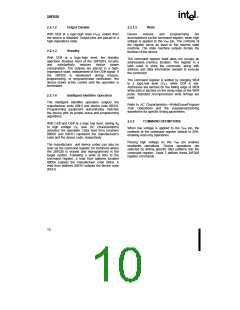
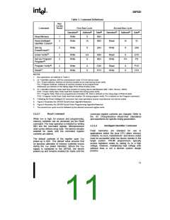
Table 3. Command Definitions
Bus
Cycles
Req’d
Command
First Bus Cycle
Second Bus Cycle
Operation(1)
Write
Address(2)
Data(3)
00H
Operation(1)
Address(2)
Data(3)
Read Memory
1
3
X
Read Intelligent
Identifier Codes(4)
Write
IA
90H
Read
Write
IA
X
ID
Set-Up
2
Write
X
20H
20H
Erase/Erase(5)
Erase Verify(5)
2
2
Write
Write
EA
X
A0H
40H
Read
Write
X
EVD
PD
Set-Up Program/
Program(6)
PA
Program Verify(6)
2
2
Write
Write
X
X
C0H
FFH
Read
Write
X
X
PVD
FFH
Reset(7)
NOTES:
1. Bus operations are defined in Table 2.
2. IA = Identifier address: 00H for manufacturer code, 01H for device code.
EA = Erase Address: Address of memory location to be read during erase verify.
PA = Program Address: Address of memory location to be programmed.
Addresses are latched on the falling edge of the Write-Enable pulse.
3. ID = Identifier Address: Data read from location IA during device identification (Mfr = 89H, Device = BDH).
EVD = Erase Verify Data: Data read from location EA during erase verify.
PD = Program Data: Data to be programmed at location PA. Data is latched on the rising edge of Write-Enable.
PVD = Program Verify Data: Data read from location PA during program verify. PA is latched on the Program command.
4. Following the Read Intelligent ID command, two read operations access manufacturer and device codes.
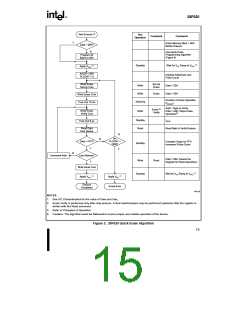
5. Figure 5 illustrates the 28F020 Quick-Erase Algorithm flowchart.
6. Figure 4 illustrates the 28F020 Quick-Pulse Programming Algorithm flowchart.
7. The second bus cycle must be followed by the desired command register write.
2.2.2.1
Read Command
command register contents are changed. Refer to
the AC Characteristics—Read-Only Operations
and waveforms for specific timing parameters.
While VPP is high, for erasure and programming,
memory contents can be accessed via the Read
command. The read operation is initiated by writing
00H into the command register. Microprocessor
read cycles retrieve array data. The device remains
enabled for reads until the command register
contents are altered.
2.2.2.2
Intelligent Identifier Command
Flash memories are intended for use in
applications where the local CPU alters memory
contents. As such, manufacturer and device codes
must be accessible while the device resides in the
target system. PROM programmers typically
access signature codes by raising A9 to a high
voltage. However, multiplexing high voltage onto
address lines is not a desired system design
practice.
The default contents of the register upon VPP
power-up is 00H. This default value ensures that
no spurious alteration of memory contents occurs
during the VPP power transition. Where the VPP
supply is hardwired to the 28F020, the device
powers-up and remains enabled for reads until the
11

 INTEL [ INTEL ]