28F020
2.2.1.2
E
Output Disable
2.2.1.5
Write
With OE# at a logic-high level (VIH), output from
the device is disabled. Output pins are placed in a
high-impedance state.
Device
erasure
and
programming
are
accomplished via the command register, when high
voltage is applied to the VPP pin. The contents of
the register serve as input to the internal state
machine. The state machine outputs dictate the
function of the device.
2.2.1.3
Standby
logic-high level, the standby
With CE# at
operation disables most of the 28F020’s circuitry
and substantially reduces device power
consumption. The outputs are placed in a high-
impedance state, independent of the OE# signal. If
the 28F020 is deselected during erasure,
programming, or program/erase verification, the
device draws active current until the operation is
terminated.
a
The command register itself does not occupy an
addressable memory location. The register is a
latch used to store the command, along with
address and data information needed to execute
the command.
The command register is written by bringing WE#
to
a logic-low level (VIL), while CE# is low.
Addresses are latched on the falling edge of WE#
while data is latched on the rising edge of the WE#
pulse. Standard microprocessor write timings are
used.
2.2.1.4
Intelligent Identifier Operation
The intelligent identifier operation outputs the
manufacturer code (89H) and device code (BDH).
Programming equipment automatically matches
the device with its proper erase and programming
algorithms.
Refer to AC Characteristics—Write/Erase/Program
Only Operations and the erase/programming
waveforms for specific timing parameters.
2.2.2
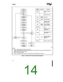
COMMAND DEFINITIONS
With CE# and OE# at a logic low level, raising A9
to high voltage VID (see DC Characteristics)
activates the operation. Data read from locations
0000H and 0001H represent the manufacturer’s
code and the device code, respectively.
When low voltage is applied to the VPP pin, the
contents of the command register default to 00H,
enabling read only operations.
Placing high voltage on the VPP pin enables
read/write operations. Device operations are
selected by writing specific data patterns into the
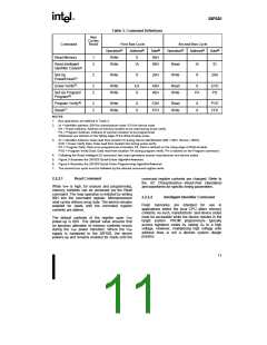
command register. Table 3 defines these 28F020
register commands.
The manufacturer and device codes can also be
read via the command register, for instances where
the 28F020 is erased and reprogrammed in the
target system. Following a write of 90H to the
command register, a read from address location
0000H outputs the manufacturer code (89H). A
read from address 0001H outputs the device code
(BDH).
10

 INTEL [ INTEL ]