28F020
E
The 28F020 contains an intelligent identifier
operation to supplement traditional PROM-
programming methodology. The operation is
initiated by writing 90H into the command register.
Following the command Write, a read cycle from
address 0000H retrieves the manufacturer code of
89H. A read cycle from address 0001H returns the
device code of BDH. To terminate the operation, it
is necessary to write another valid command into
the register.
In the case where the data read is not FFH,
another erase operation is performed. (Refer to
Section 2.2.2.3, Set-Up Erase/Erase Commands.)
Verification then resumes from the address of the
last verified byte. Once all bytes in the array have
been verified, the erase step is complete. The
device can be programmed. At this point, the verify
operation is terminated by writing a valid command
(e.g., Program Set-Up) to the command register.
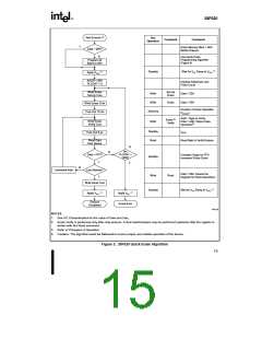
Figure 5, the 28F020 Quick-Erase Algorithm
flowchart, illustrates how commands and bus
operations are combined to perform electrical
erasure of the 28F020. Refer to AC
Characteristics—Write/Erase/Program Only Oper-
ations and waveforms for specific timing
parameters.
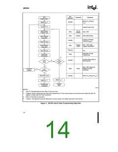
2.2.2.3
Set-Up Erase/Erase Commands
Set-Up Erase is a command-only operation that
stages the device for electrical erasure of all bytes
in the array. The set-up erase operation is
performed by writing 20H to the command register.
2.2.2.5
Set-Up Program/Program
Commands
To commence chip-erasure, the Erase command
(20H) must again be written to the register. The
erase operation begins with the rising edge of the
WE# pulse and terminates with the rising edge of
the next WE# pulse (i.e., Erase Verify command).
Set-Up program is a command-only operation that
stages the device for byte programming. Writing
40H into the command register performs the set-up
operation.
This two-step sequence of set-up followed by
execution ensures that memory contents are not
accidentally erased. Also, chip-erasure can only
occur when high voltage is applied to the VPP pin.
In the absence of this high voltage, memory
contents are protected against erasure. Refer to
AC Characteristics—Write/Erase/Program Only
Operations and waveforms for specific timing
parameters.
Once the program set-up operation is performed,
the next WE# pulse causes a transition to an active
programming operation. Addresses are internally
latched on the falling edge of the WE# pulse. Data
is internally latched on the rising edge of the WE#
pulse. The rising edge of WE# also begins the
programming
operation.
The
programming
operation terminates with the next rising edge of
WE# used to write the Program Verify command.
Refer to AC Characteristics—Write/Erase/Program
Only Operations and waveforms for specific timing
parameters.
2.2.2.4
Erase Verify Command
The Erase command erases all bytes of the array
in parallel. After each erase operation, all bytes
must be verified. The erase verify operation is
initiated by writing A0H into the command register.
The address for the byte to be verified must be
supplied as it is latched on the falling edge of the
WE# pulse. The register write terminates the erase
operation with the rising edge of its WE# pulse.
2.2.2.6
Program Verify Command
The 28F020 is programmed on a byte-by-byte
basis. Byte programming may occur sequentially or
at random. Following each programming operation,
the byte just programmed must be verified.
The program verify operation is initiated by writing
C0H into the command register. The register write
terminates the programming operation with the
rising edge of its WE# pulse. The program verify
operation stages the device for verification of the
byte last programmed. No new address information
is latched.
The 28F020 applies an internally-generated margin
voltage to the addressed byte. Reading FFH from
the addressed byte indicates that all bits in the byte
are erased.
The Erase Verify command must be written to the
command register prior to each byte verification to
latch its address. The process continues for each
byte in the array until a byte does not return FFH
data, or the last address is accessed.
The 28F020 applies an internally-generated margin
voltage to the byte. A microprocessor read cycle
outputs the data.
A
successful comparison
12

 INTEL [ INTEL ]