28F020
E
VCC
VPP
VCC
80C186
System Bus
VCC
VPP
VCC
A1-A18
DQ8 -DQ15
DQ0 -DQ7
A0-A17
A0-A17
DQ0-DQ7
DQ0-DQ7
28F020
28F020
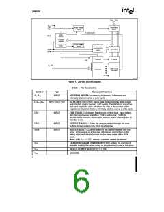
Address Decoded
Chip Select
CE#
CE#
BHE#
WR#
A0
WE#
WE#
OE#
RD#
OE#
0245_03
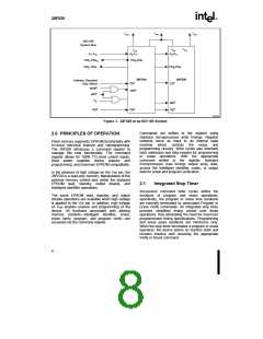
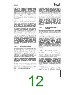
Figure 3. 28F020 in an 80C186 System
Commands are written to the register using
standard microprocessor write timings. Register
contents serve as input to an internal state
machine which controls the erase and
programming circuitry. Write cycles also internally
latch addresses and data needed for programming
or erase operations. With the appropriate
command written to the register, standard
microprocessor read timings output array data,
access the intelligent identifier codes, or output
data for erase and program verification.
2.0 PRINCIPLES OF OPERATION
Flash memory augments EPROM functionality with
in-circuit electrical erasure and reprogramming.
The 28F020 introduces a command register to
manage this new functionality. The command
register allows for 100% TTL-level control inputs,
fixed power supplies during erasure and
programming, and maximum EPROM compatibility.
In the absence of high voltage on the VPP pin, the
28F020 is a read-only memory. Manipulation of the
external memory control pins yields the standard
EPROM read, standby, output disable, and
intelligent identifier operations.
2.1
Integrated Stop Timer
Successive command write cycles define the
durations of program and erase operations;
specifically, the program or erase time durations
are normally terminated by associated Program or
Erase Verify commands. An integrated stop timer
provides simplified timing control over these
operations; thus eliminating the need for maximum
program/erase timing specifications. Programming
and erase pulse durations are minimums only.
When the stop timer terminates a program or erase
operation, the device enters an inactive state and
remains inactive until receiving the appropriate
Verify or Reset command.
The same EPROM read, standby, and output
disable operations are available when high voltage
is applied to the VPP pin. In addition, high voltage
on VPP enables erasure and programming of the
device. All functions associated with altering
memory contents—intelligent identifier, erase,
erase verify, program, and program verify—are
accessed via the command register.
8

 INTEL [ INTEL ]