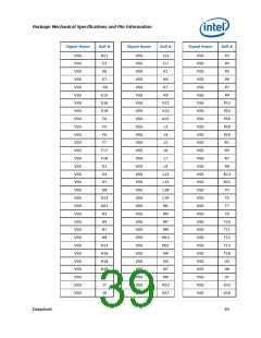
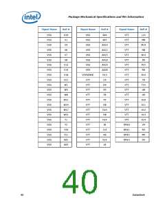
Package Mechanical Specifications and Pin Information
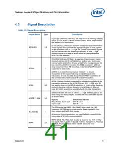
Signal Name
Type
Description
DBSY# (Data Bus Busy) is asserted by the agent responsible for
driving data on the FSB to indicate that the data bus is in use.
The data bus is released after DBSY# is de-asserted. This signal
must connect the appropriate pins on both FSB agents.
DBSY#
I/O
DEFER# is asserted by an agent to indicate that a transaction
cannot be guaranteed in-order completion. Assertion of DEFER#
is normally the responsibility of the addressed memory or
Input/Output agent. This signal must connect the appropriate
pins of both FSB agents.
DEFER#
I
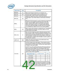
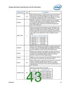
DINV [3:0]# (Data Bus Inversion) are source synchronous and
indicate the polarity of the D [63:0]# signals. The DINV [3:0]#
signals are activated when the data on the data bus is inverted.
The bus agent will invert the data bus signals if more than half
the bits, within the covered group, would change level in the next
cycle. DINV [3:0]# assignment to data bus signals is shown
below.
DINV [3:0]#
I
Bus Signal
Data Bus Signals
DINV [3]#
DINV [2]#
DINV [1]#
DINV [0]#
D [63:48]#
D [47:32]#
D [31:16]#
D [15:0]#
DPRSTP# when asserted on the platform causes the processor to
transition from the Deep Sleep State to the Deeper Sleep state.
In order to return to the Deep Sleep State, DPRSTP# must be de-
asserted. DPRSTP# is driven by the South Bridge chipset.
DPRSTP#
I
DPSLP# when asserted on the platform causes the processor to
transition from the Sleep State to the Deep Sleep state. In order
to return to the Sleep State, DPSLP# must be de-asserted.
DPSLP# is driven by the South Bridge chipset.
DPSLP#
DPWR#
I
I
DPWR# is a control signal from the Intel 945GSE chipset used to
reduce power on the processor data bus input buffers.
DRDY# (Data Ready) is asserted by the data driver on each data
transfer, indicating valid data on the data bus. In a multi-
common clock data transfer, DRDY# may be de-asserted to
insert idle clocks. This signal must connect the appropriate pins of
both FSB agents.
DRDY#
I/O
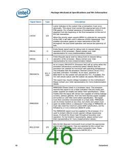
Data strobe used to latch in D [63:0]#
Signals
Associated Strobe
D [15:0]#
D [31:16]#
D [47:32]#
D [63:48]#
DINV [0]#, DSTBN [0]#
DINV [1]#, DSTBN [1]#
DINV [2]#, DSTBN [2]#
DINV [3]#, DSTBN [3]#
DSTBN [3:0]#
I/O
Datasheet
43

 INTEL [ INTEL ]