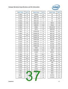
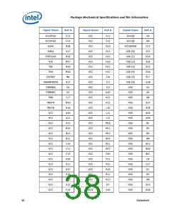
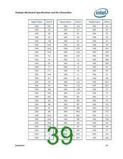
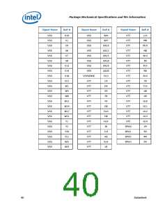
Package Mechanical Specifications and Pin Information
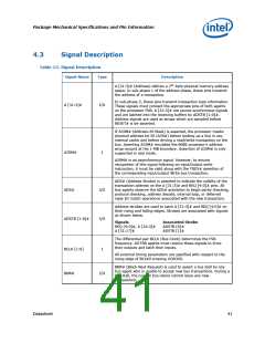
4.3
Signal Description
Table 13. Signal Description
Signal Name
Type
Description
A [31:3]# (Address) defines a 232-byte physical memory address
space. In sub-phase 1 of the address phase, these pins transmit
the address of a transaction.
In sub-phase 2, these pins transmit transaction type information.
These signals must connect the appropriate pins of both agents
on the processor FSB. A [31:3]# are source synchronous signals
and are latched into the receiving buffers by ADSTB [1:0]#.
Address signals are used as straps which are sampled before
RESET# is de-asserted.
A [31:3]#
I/O
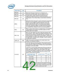
If A20M# (Address-20 Mask) is asserted, the processor masks
physical address bit 20 (A20#) before looking up a line in any
internal cache and before driving a read/write transaction on the
bus. Asserting A20M# emulates the 8086 processor's address
wrap-around at the 1-MB boundary. Assertion of A20M# is only
supported in real mode.
A20M#
I
A20M# is an asynchronous signal. However, to ensure
recognition of this signal following an input/output write
instruction, it must be valid along with the TRDY# assertion of
the corresponding input/output Write bus transaction.
ADS# (Address Strobe) is asserted to indicate the validity of the
transaction address on the A [31:3]# and REQ [4:0]# pins. All
bus agents observe the ADS# activation to begin parity checking,
protocol checking, address decode, internal loop, or deferred
reply ID match operations associated with the new transaction.
ADS#
I/O
I/O
Address strobes are used to latch A [31:3]# and REQ [4:0]# on
their rising and falling edges. Strobes are associated with signals
as shown below.
ADSTB [1:0]#
Signals
REQ [4:0]#, A [16:3]#
A [31:17]#
Associated Strobe
ADSTB [0]#
ADSTB [1]#
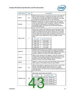
The differential pair BCLK (Bus Clock) determines the FSB
frequency. All FSB agents must receive these signals to drive
their outputs and latch their inputs.
BCLK [1:0]
BNR#
I
All external timing parameters are specified with respect to the
rising edge of BCLK0 crossing VCROSS.
BNR# (Block Next Request) is used to assert a bus stall by any
bus agent who is unable to accept new bus transactions. During a
bus stall, the current bus owner cannot issue any new
transactions.
I/O
Datasheet
41

 INTEL [ INTEL ]