1-Gbit P30 Family
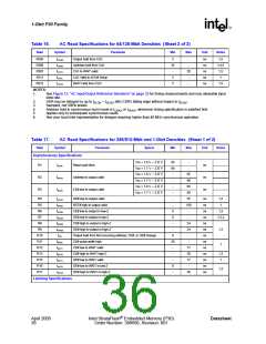
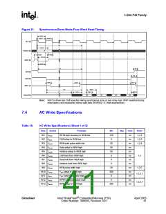
Table 17.
AC Read Specifications for 256/512-Mbit and 1-Gbit Densities (Sheet 2 of 2)
Num
Symbol
Parameter
Speed
Min
Max
Unit
Notes
R101
R102
tAVVH
tELVH
Address setup to ADV# high
CE# low to ADV# high
10
10
-
-
-
ns
ns
Vcc = 1.8 V – 2.0 V
Vcc = 1.7 V – 2.0 V
85
88
-
R103
tVLQV
ADV# low to output valid
ns
1
-
R104
R105
R106
R108
R111
tVLVH
tVHVL
tVHAX
tAPA
ADV# pulse width low
10
10
9
ns
ns
ns
ns
ns
ADV# pulse width high
Address hold from ADV# high
Page address access
-
-
1,4
1
-
25
-
tphvh
RST# high to ADV# high
30
Clock Specifications
R200
R201
R202
R203
fCLK
tCLK
CLK frequency
CLK period
-
25
5
40
-
MHz
ns
1,3,6
tCH/CL
CLK high/low time
CLK fall/rise time
-
ns
tFCLK/RCLK
-
3
ns
Synchronous Specifications
R301
R302
R303
R304
R305
R306
R307
R311
R312
tAVCH/L
tVLCH/L
tELCH/L
CHQV / tCLQV
tCHQX
Address setup to CLK
ADV# low setup to CLK
CE# low setup to CLK
CLK to output valid
9
9
9
-
-
-
ns
ns
ns
ns
ns
ns
ns
ns
ns
1
-
t
20
-
Output hold from CLK
Address hold from CLK
CLK to WAIT valid
3
10
-
1,5
1,4,5
1,5
1
tCHAX
-
tCHTV
20
-
tCHVL
CLK Valid to ADV# Setup
WAIT Hold from CLK
3
3
tCHTX
-
1,5
NOTES:
1.
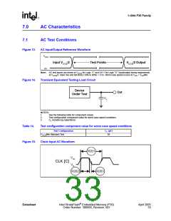
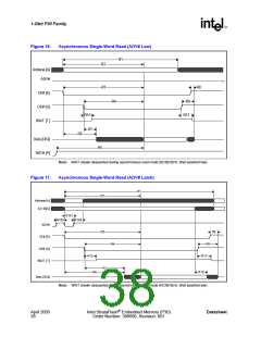
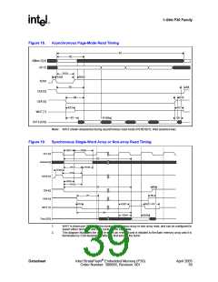
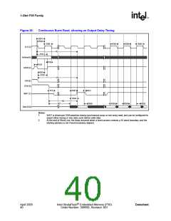
See Figure 13, “AC Input/Output Reference Waveform” on page 33 for timing measurements and max allowable input
slew rate.
2.
3.
4.
5.
6.
OE# may be delayed by up to t
Sampled, not 100% tested.
Address hold in synchronous burst mode is t
Applies only to subsequent synchronous reads.
See your local Intel representative for designs requiring higher than 40 MHz synchronous operation.
– t
after CE#’s falling edge without impact to t
.
ELQV
GLQV
ELQV
or t
, whichever timing specification is satisfied first.
VHAX
CHAX
Datasheet
Intel StrataFlash® Embedded Memory (P30)
Order Number: 306666, Revision: 001
April 2005
37

 INTEL [ INTEL ]