1-Gbit P30 Family
7.0
AC Characteristics
7.1
AC Test Conditions
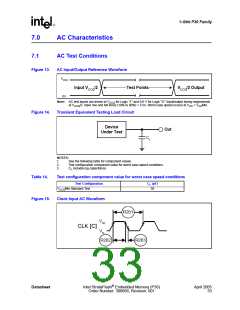
Figure 13.
AC Input/Output Reference Waveform
VCCQ
Input VCCQ/2
Test Points
VCCQ/2 Output
Note: AC test inputs are driven at V
for Logic "1" and 0.0 V for Logic "0." Input/output timing begins/ends
CCQ
at V
/2. Input rise and fall times (10% to 90%) < 5 ns. Worst case speed occurs at V = V Min.
CCQ
CC CC
Figure 14.
Transient Equivalent Testing Load Circuit
Device
Under Test
Out
CL
NOTES:
1.
2.
3.
See the following table for component values.
Test configuration component value for worst case speed conditions.
C includes jig capacitance
L
.
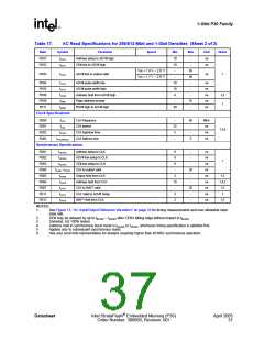
Table 14.
Test configuration component value for worst case speed conditions
Test Configuration
Min Standard Test
C (pF)
L
V
30
CCQ
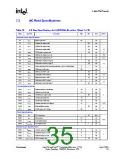
Figure 15.
Clock Input AC Waveform
R201
VIH
CLK [C]
VIL
R202
R203
Datasheet
Intel StrataFlash® Embedded Memory (P30)
Order Number: 306666, Revision: 001
April 2005
33

 INTEL [ INTEL ]