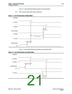
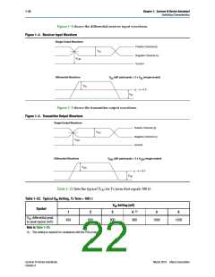
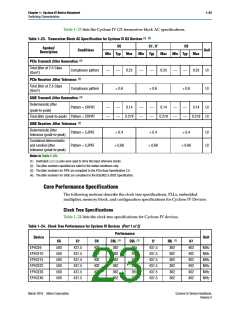
Chapter 1: Cyclone IV Device Datasheet
1–25
Switching Characteristics
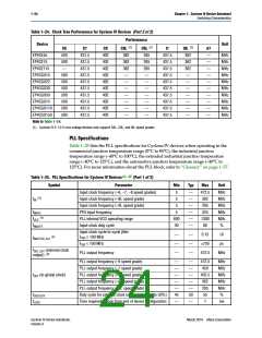
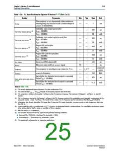
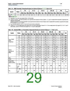
Table 1–25. PLL Specifications for Cyclone IV Devices (1), (2) (Part 2 of 2)
Symbol
Parameter
Min
Typ
Max
Unit
Time required to lock dynamically (after switchover,
reconfiguring any non-post-scale counters/delays or
areset is deasserted)
tDLOCK
—
—
1
ms
Dedicated clock output period jitter
—
—
—
—
—
—
—
—
—
—
—
—
—
—
300
30
ps
mUI
ps
(6)
FOUT 100 MHz
tOUTJITTER_PERIOD_DEDCLK
FOUT < 100 MHz
Dedicated clock output cycle-to-cycle jitter
300
30
(6)
FOUT 100 MHz
tOUTJITTER_CCJ_DEDCLK
FOUT < 100 MHz
mUI
ps
Regular I/O period jitter
OUT 100 MHz
650
75
(6)
F
tOUTJITTER_PERIOD_IO
FOUT < 100 MHz
mUI
ps
Regular I/O cycle-to-cycle jitter
650
(6)
FOUT 100 MHz
tOUTJITTER_CCJ_IO
F
OUT < 100 MHz
—
—
10
—
—
—
75
50
—
mUI
ps
tPLL_PSERR
tARESET
Accuracy of PLL phase shift
Minimum pulse width on areset signal.
ns
SCANCLK
cycles
(7)
tCONFIGPLL
fSCANCLK
Time required to reconfigure scan chains for PLLs
—
—
—
3.5
—
scanclk frequency
—
—
100
425
MHz
Period jitter for dedicated clock output in cascaded
PLLs (FOUT 100 MHz)
ps
tCASC_OUTJITTER_PERIOD_DEDCLK
(8), (9)
Period jitter for dedicated clock output in cascaded
PLLs (FOUT 100 MHz)
—
—
42.5
mUI
Notes to Table 1–25:
(1) This table is applicable for general purpose PLLs and multipurpose PLLs.
(2) You must connect VCCD_PLL to VCCINT through the decoupling capacitor and ferrite bead.
(3) This parameter is limited in the Quartus II software by the I/O maximum frequency. The maximum I/O frequency is different for each I/O
standard.
(4) The VCO frequency reported by the Quartus II software in the PLL Summary section of the compilation report takes into consideration the VCO
post-scale counter K value. Therefore, if the counter K has a value of 2, the frequency reported can be lower than the fVCO specification.
(5) A high input jitter directly affects the PLL output jitter. To have low PLL output clock jitter, you must provide a clean clock source that is less
than 200 ps.
(6) Peak-to-peak jitter with a probability level of 10–12 (14 sigma, 99.99999999974404% confidence level). The output jitter specification applies
to the intrinsic jitter of the PLL when an input jitter of 30 ps is applied.
(7) With 100-MHz scanclk frequency.
(8) The cascaded PLLs specification is applicable only with the following conditions:
■
Upstream PLL—0.59 MHz Upstream PLL bandwidth < 1 MHz
■
Downstream PLL—Downstream PLL bandwidth > 2 MHz
(9) PLL cascading is not supported for transceiver applications.
March 2016 Altera Corporation
Cyclone IV Device Handbook,
Volume 3

 INTEL [ INTEL ]