Chapter 1: Cyclone IV Device Datasheet
1–27
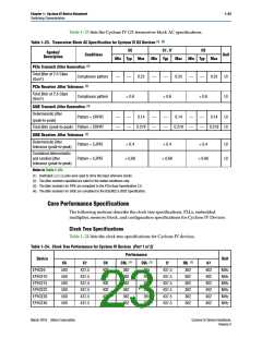
Switching Characteristics
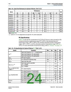
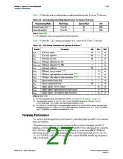
Table 1–29 lists the active configuration mode specifications for Cyclone IV devices.
Table 1–29. Active Configuration Mode Specifications for Cyclone IV Devices
Programming Mode
DCLK Range
20 to 40
Typical DCLK
Unit
MHz
MHz
(1)
Active Parallel (AP)
33
33
Active Serial (AS)
20 to 40
Note to Table 1–29:
(1) AP configuration mode is only supported for Cyclone IV E devices.
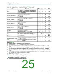
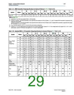
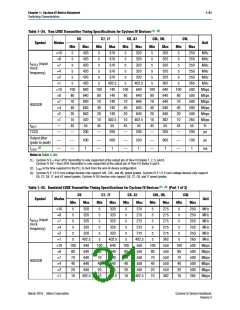
Table 1–30 lists the JTAG timing parameters and values for Cyclone IV devices.
Table 1–30. JTAG Timing Parameters for Cyclone IV Devices (1)
Symbol
tJCP
Parameter
Min
40
19
19
1
Max
—
—
—
—
—
—
15
15
15
—
—
25
25
25
Unit
ns
ns
ns
ns
ns
ns
ns
ns
ns
ns
ns
ns
ns
ns
TCK clock period
tJCH
TCK clock high time
TCK clock low time
tJCL
tJPSU_TDI JTAG port setup time for TDI
tJPSU_TMS JTAG port setup time for TMS
3
tJPH
JTAG port hold time
10
—
—
—
5
(2), (3)
tJPCO
tJPZX
tJPXZ
tJSSU
tJSH
JTAG port clock to output
(2), (3)
(2), (3)
JTAG port high impedance to valid output
JTAG port valid output to high impedance
Capture register setup time
Capture register hold time
10
—
—
—
tJSCO
tJSZX
tJSXZ
Update register clock to output
Update register high impedance to valid output
Update register valid output to high impedance
Notes to Table 1–30:
(1) For more information about JTAG waveforms, refer to “JTAG Waveform” in “Glossary” on page 1–37.
(2) The specification is shown for 3.3-, 3.0-, and 2.5-V LVTTL/LVCMOS operation of JTAG pins. For 1.8-V
LVTTL/LVCMOS and 1.5-V LVCMOS, the output time specification is 16 ns.
(3) For EP4CGX22, EP4CGX30 (F324 and smaller package), EP4CGX110, and EP4CGX150 devices, the output time
specification for 3.3-, 3.0-, and 2.5-V LVTTL/LVCMOS operation of JTAG pins is 16 ns. For 1.8-V LVTTL/LVCMOS
and 1.5-V LVCMOS, the output time specification is 18 ns.
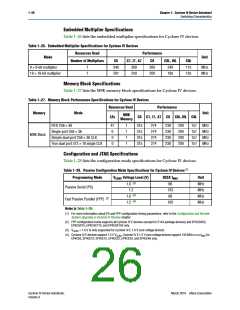
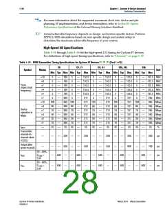
Periphery Performance
This section describes periphery performance, including high-speed I/O and external
memory interface.
I/O performance supports several system interfaces, such as the high-speed I/O
interface, external memory interface, and the PCI/PCI-X bus interface. I/Os using the
SSTL-18 Class I termination standard can achieve up to the stated DDR2 SDRAM
interfacing speeds. I/Os using general-purpose I/O standards such as 3.3-, 3.0-, 2.5-,
1.8-, or 1.5-LVTTL/LVCMOS are capable of a typical 200 MHz interfacing frequency
with a 10 pF load.
March 2016 Altera Corporation
Cyclone IV Device Handbook,
Volume 3

 INTEL [ INTEL ]