®
MOBILE PENTIUM PROCESSOR WITH MMX™ TECHNOLOGY
WARNING
4.0. ELECTRICAL SPECIFICATIONS
4.1. Absolute Maximum Ratings
Stressing the device beyond the "Absolute
Maximum Ratings" may cause permanent damage.
These are stress ratings only. Operation beyond the
"Operating Conditions" is not recommended and
extended exposure beyond the "Operating
Conditions" may affect device reliability.
The following values are stress ratings only.
Functional operation at the maximum ratings is not
implied nor guaranteed. Functional operating
conditions are given in the AC and DC specification
tables.
4.2.
DC Specifications
Extended exposure to the maximum ratings may
affect device reliability. Furthermore, although the
mobile Pentium processor with MMX technology
contains protective circuitry to resist damage from
Electrostatic Discharge (ESD), always take
precautions to avoid high static voltages or electric
fields.
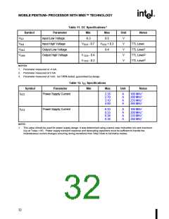
Tables 10, 11, 12 and 13 list the DC specifications
which apply to the mobile Pentium processor with
MMX technology on 0.25 Micron. The processor
core operates at 1.8V (166/200/233 MHz) or 2.0V
(266 MHz) internally while the I/O interface
operates at 2.5V.
Case temperature under bias .........- 65°C to 110°C
Storage temperature.......................- 65°C to 150°C
4.2.1.
POWER SEQUENCING
There is no specific sequence required for powering
up or powering down the VCC2 and VCC3 power
supplies. However, for compatibility with future
mobile processors, it is recommended that the VCC2
and VCC3 power supplies be either both ON or both
OFF within one second of each other.
VCC3 Supply voltage
with respect to VSS ..........................- 0.5V to +3.2V
VCC2 Supply voltage
with respect to VSS ..........................- 0.5V to +2.8V
2.5V Only Buffer DC Input
Voltage...................................- 0.5V to VCC3+0.5V*
*not to exceed V CC3 max
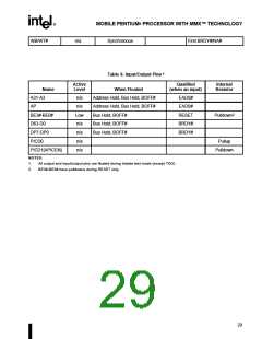
Table 10. VCC and TCASE Specifications
Package
TCP
TCASE
Supply
Min Voltage Max Voltage
Voltage
Frequency
Tolerance
0 to 95ºC
VCC2
1.665V
1.850V
2.375V
1.935V
2.150V
2.625V
1.8V +/- 0.135V
2.0V +/- 0.150V
2.5V +/- 0.125V
166/200/233 MHz
266 MHz
VCC3
166/200/233/266 MHz
31

 INTEL [ INTEL ]