®
MOBILE PENTIUM PROCESSOR WITH MMX™ TECHNOLOGY
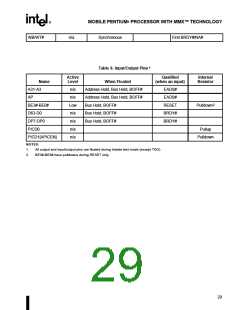
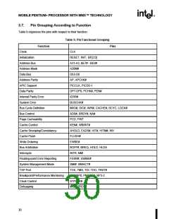
3.7. Pin Grouping According to Function
Table 9 organizes the pins with respect to their function.
Table 9. Pin Functional Grouping
Function
Pins
Clock
CLK
Initialization
Address Bus
Address Mask
Data Bus
RESET, INIT, BF[2:0]
A31-A3, BE7# - BE0#
A20M#
D63-D0
Address Parity
APIC Support
Data Parity
AP, APCHK#
PICCLK, PICD0-1
DP7-DP0, PCHK#, PEN#
IERR#
Internal Parity Error
System Error
BUSCHK#
Bus Cycle Definition
Bus Control
M/IO#, D/C#, W/R#, CACHE#, SCYC, LOCK#
ADS#, BRDY#, NA#
PCD, PWT
Page Cacheability
Cache Control
KEN#, WB/WT#
Cache Snooping/Consistency
Cache Flush
AHOLD, EADS#, HIT#, HITM#, INV
FLUSH#
Write Ordering
EWBE#
Bus Arbitration
BOFF#, BREQ, HOLD, HLDA
INTR, NMI
Interrupts
Floating-point Error Reporting
System Management Mode
TAP Port
FERR#, IGNNE#
SMI#, SMIACT#
TCK, TMS, TDI, TDO, TRST#
PM0/BP0, PM1/BP1, BP3-2
STPCLK#
Breakpoint/Performance Monitoring
Clock Control
Debugging
R/S#, PRDY
30

 INTEL [ INTEL ]