Processor Configuration Registers
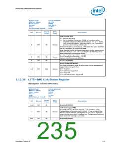
B/D/F/Type:
Address Offset:
Reset Value:
Access:
0/0/0/DMIBAR
88–89h
0000h
RW, RW-V
16 bits
Size:
BIOS Optimal Default
000h
Reset
Value
RST/
PWR
Bit
Access
Description
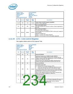
Link Disable (LD)
0 = Normal operation
1 = link is disabled. Forces the LTSSM to transition to the
Disabled state (using Recovery) from L0, L0s, or L1 states.
Link retraining happens automatically on 0 to 1 transition,
just like when coming out of reset.
Writes to this bit are immediately reflected in the value read from
the bit, regardless of actual Link state.
After clearing this bit, software must honor timing requirements
defined in Section 6.6.1 with respect to the first Configuration
Read following a Conventional Reset.
4
RW
0b
Uncore
Uncore
Uncore
Read Completion Boundary (RCB)
Hardwired to 0 to indicate 64 byte.
3
2
RO
RO
0b
0h
Reserved (RSVD)
Active State PM (ASPM)
This field controls the level of active state power management
supported on the given link.
00 = Disabled
1:0
RW
00b
01 = L0s Entry Supported
10 = Reserved
11 = L0s and L1 Entry Supported
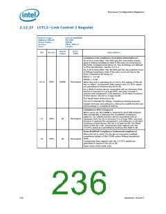
2.12.26 LSTS—DMI Link Status Register
This register indicates DMI status.
B/D/F/Type:
Address Offset:
Reset Value:
Access:
0/0/0/DMIBAR
8A–8Bh
0001h
RO-V
16 bits
Size:
BIOS Optimal Default
00h
Reset
Value
RST/
PWR
Bit
Access
Description
15:12
RO
0h
0b
0h
Reserved (RSVD)
Link Training (LTRN)
This field indicates that the Physical Layer LTSSM is in the
Configuration or Recovery state, or that 1b was written to the
Retrain Link bit but Link training has not yet begun. Hardware
clears this bit when the LTSSM exits the Configuration/Recovery
state once Link training is complete.
11
RO-V
RO
Uncore
10:0
Reserved (RSVD)
Datasheet, Volume 2
235

 INTEL [ INTEL ]