Processor Configuration Registers
2.12.23 DMILE2A—DMI Link Entry 2 Address Register
This register provides the second part of a Link Entry that declares an internal link to
another Root Complex Element.
B/D/F/Type:
Address Offset:
Reset Value:
Access:
0/0/0/DMIBAR
68–6Bh
00000000h
RW-O
32 bits
000h
Size:
BIOS Optimal Default
Reset
Value
RST/
PWR
Bit
Access
Description
Link Address (LA)
31:12
11:0
RW-O
RO
00000h
0h
Uncore
Memory mapped base address of the RCRB that is the target
element (Egress Port) for this link entry.
Reserved (RSVD)
2.12.24 LCAP—Link Capabilities Register
This register indicates DMI specific capabilities.
B/D/F/Type:
Address Offset:
Reset Value:
Access:
0/0/0/DMIBAR
84–87h
0001AC41h
RW-O, RO, RW-OV
32 bits
Size:
BIOS Optimal Default
00002h
Reset
Value
RST/
PWR
Bit
Access
Description
31:18
RO
0h
Reserved (RSVD)
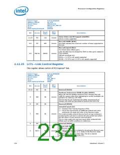
L1 Exit Latency (L1SELAT)
This field indicates the length of time this Port requires to
complete the transition from L1 to L0. The value 011b indicates
the range of 4 us to less than 8 us.
000 = Less than 1µs
001 = 1 µs to less than 2 µs
010 = 2 µs to less than 4 µs
011 = 4 µs to less than 8 µs
100 = 8 µs to less than 16 µs
101 = 16 µs to less than 32 µs
110 = 32 µs-64 µs
17:15
RW-O
011b
Uncore
111 = More than 64 µs
Both bytes of this register that contain a portion of this field must
be written simultaneously in order to prevent an intermediate
(and undesired) value from ever existing.
L0s Exit Latency (L0SELAT)
This field indicates the length of time this Port requires to
complete the transition from L0s to L0.
000 = Less than 64 ns
001 = 64 ns to less than 128 ns
010 = 128 ns to less than 256 ns
011 = 256 ns to less than 512 ns
100 = 512 ns to less than 1 µs
101 = 1 µs to less than 2 µs
110 = 2 µs-4 µs
14:12
RW-O
010b
Uncore
111 = More than 4 µs
Datasheet, Volume 2
233

 INTEL [ INTEL ]