Processor Configuration Registers
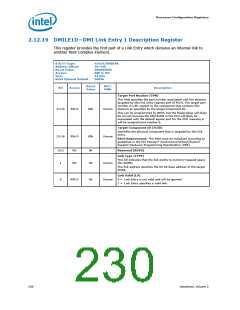
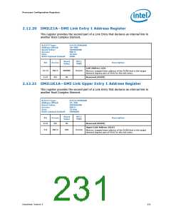
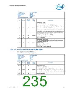
2.12.20 DMILE1A—DMI Link Entry 1 Address Register
This register provides the second part of a Link Entry that declares an internal link to
another Root Complex Element.
B/D/F/Type:
Address Offset:
Reset Value:
Access:
0/0/0/DMIBAR
58–5Bh
00000000h
RW-O
32 bits
000h
Size:
BIOS Optimal Default
Reset
Value
RST/
PWR
Bit
Access
Description
Link Address (LA)
31:12
11:0
RW-O
RO
00000h
0h
Uncore
Memory mapped base address of the RCRB that is the target
element (egress port of PCH) for this link entry.
Reserved (RSVD)
2.12.21 DMILUE1A—DMI Link Upper Entry 1 Address Register
This register provides the second part of a Link Entry that declares an internal link to
another Root Complex Element.
B/D/F/Type:
Address Offset:
Reset Value:
Access:
0/0/0/DMIBAR
5C–5Fh
00000000h
RW-O
32 bits
000000h
Size:
BIOS Optimal Default
Reset
Value
RST/
PWR
Bit
Access
Description
31:8
RO
0h
Reserved (RSVD)
Upper Link Address (ULA)
7:0
RW-O
00h
Uncore
Memory mapped base address of the RCRB that is the target
element (egress port of PCH) for this link entry.
Datasheet, Volume 2
231

 INTEL [ INTEL ]