Processor Configuration Registers
2.6.48
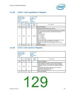
LCAP2—Link Capabilities 2 Register
B/D/F/Type:
Address Offset:
Reset Value:
Access:
0/1/0–2/MMR
CC–CFh
0000000Eh
RO-V
32 bits
0000000h
Size:
BIOS Optimal Default
Reset
Value
RST/
PWR
Bit
Access
Description
31:8
RO
0h
07h
0h
Reserved (RSVD)
Supported Link Speeds Vector (SLSV)
This field indicates the supported Link speed(s) of the associated
Port. For each bit, a value of 1b indicates that the corresponding
Link speed is supported; otherwise, the Link speed is not
supported.
Bit definitions are:
Bit 1 = 2.5 GT/s
Bit 2 = 5.0 GT/s
Bit 3 = 8.0 GT/s
Bits 7:4 = Reserved
Multi-Function devices associated with an Upstream Port must
report the same value in this field for all Functions.
DMI does not support this control register since it is Gen3
register.
7:1
RO-V
Uncore
0
RO
Reserved (RSVD)
2.6.49
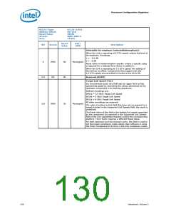
LCTL2—Link Control 2 Register
B/D/F/Type:
Address Offset:
Reset Value:
Access:
0/1/0–2/PCI
D0–D1h
0003h
RWS, RWS-V
16 bits
Size:
Reset
Value
RST/
PWR
Bit
Access
Description
15:11
RO
0h
0b
0h
Reserved (RSVD)
Enter Modified Compliance (entermodcompliance)
When this bit is set to 1b, the device transmits modified
compliance pattern if the LTSSM enters Polling.Compliance
state.
Components that support only the 2.5 GT/s speed are
permitted to hardwire this bit to 0b.
10
RWS
RO
Powergood
Reset Value of this field is 0b.
9:7
Reserved (RSVD)
Datasheet, Volume 2
129

 INTEL [ INTEL ]