Processor Configuration Registers
2.6.30
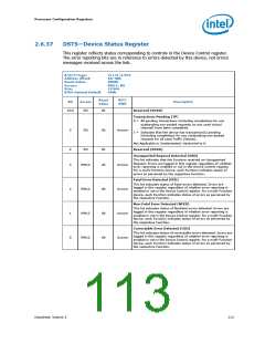
MC—Message Control Register
System software can modify bits in this register, but the device is prohibited from doing
so.
If the device writes the same message multiple times, only one of those messages is
ensured to be serviced. If all of them must be serviced, the device must not generate
the same message again until the driver services the earlier one.
B/D/F/Type:
Address Offset:
Reset Value:
Access:
0/1/0–2/PCI
92–93h
0000h
RW, RO
16 bits
00h
Size:
BIOS Optimal Default
Reset
Value
RST/
PWR
Bit
Access
Description
15:8
RO
0h
Reserved (RSVD)
64-bit Address Capable (B64AC)
Hardwired to 0 to indicate that the function does not implement
the upper 32 bits of the Message Address register and is
incapable of generating a 64-bit memory address.
7
RO
0b
Uncore
Uncore
Multiple Message Enable (MME)
System software programs this field to indicate the actual
number of messages allocated to this device. This number will be
equal to or less than the number actually requested.
6:4
RW
000b
The encoding is the same as for the MMC field below.
Multiple Message Capable (MMC)
System software reads this field to determine the number of
messages being requested by this device.
000 = 1 Message Requested
All of the following are reserved in this implementation:
001 = 2
010 = 4
3:1
RO
000b
Uncore
011 = 8
100 = 16
101 = 32
110 = Reserved
111 = Reserved
MSI Enable (MSIEN)
This bit controls the ability of this device to generate MSIs.
0 = MSI will not be generated.
1 = MSI will be generated when we receive PME messages. INTA
will not be generated and INTA Status (PCISTS1[3]) will not
be set.
0
RW
0b
Uncore
Datasheet, Volume 2
109

 INTEL [ INTEL ]