Processor Configuration Registers
2.6.34
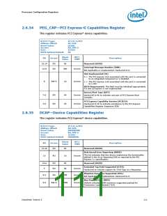
PEG_CAP—PCI Express-G Capabilities Register
This register indicates PCI Express* device capabilities.
B/D/F/Type:
Address Offset:
Reset Value:
Access:
0/1/0–2/PCI
A2–A3h
0142h
RO, RW-O
16 bits
Size:
BIOS Optimal Default
0h
Reset
Value
RST/
PWR
Bit
Access
Description
15:14
13:9
RO
RO
0h
Reserved (RSVD)
Interrupt Message Number (IMN)
Not Applicable or Implemented. Hardwired to 0.
00h
Uncore
Uncore
Slot Implemented (SI)
0 = The PCI Express Link associated with this port is connected
to an integrated component or is disabled.
1 = The PCI Express Link associated with this port is connected
to a slot.
8
RW-O
1b
BIOS Requirement: This field must be initialized appropriately
if a slot connection is not implemented.
Device/Port Type (DPT)
7:4
3:0
RO
RO
4h
2h
Uncore
Uncore
Hardwired to 4h to indicate root port of PCI Express Root
Complex.
PCI Express Capability Version (PCIECV)
Hardwired to 2h to indicate compliance to the PCI Express
Capabilities Register Expansion ECN.
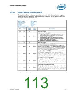
2.6.35
DCAP—Device Capabilities Register
This register indicates PCI Express* device capabilities.
B/D/F/Type:
Address Offset:
Reset Value:
Access:
0/1/0–2/PCI
A4–A7h
00008000h
RO, RW-O
32 bits
Size:
BIOS Optimal Default
0000000h
Reset
Value
RST/
PWR
Bit
Access
Description
31:16
RO
0h
Reserved (RSVD)
Role Based Error Reporting (RBER)
This bit indicates that this device implements the functionality
defined in the Error Reporting ECN as required by the PCI
Express 1.1 specification.
15
RO
1b
Uncore
14:6
5
RO
RO
0h
0b
Reserved (RSVD)
Extended Tag Field Supported (ETFS)
Hardwired to indicate support for 5-bit Tags as a Requestor.
Uncore
Uncore
Phantom Functions Supported (PFS)
Not Applicable or Implemented. Hardwired to 0.
4:3
2:0
RO
00b
Max Payload Size (MPS)
Default indicates 128B maximum supported payload for
Transaction Layer Packets (TLP).
RW-O
000b
Uncore
Datasheet, Volume 2
111

 INTEL [ INTEL ]