LPC Interface Bridge Registers (D31:F0)
13.8.3.9
GPE0_STS—General Purpose Event 0 Status Register
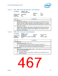
I/O Address:
PMBASE + 20h
(ACPI GPE0_BLK)
Attribute:
Bits 0:32 R/WC
Bits 33:63 RO
64-bit
Default Value:
Lockable:
Power Well:
0000000000000000h
No
Resume
Size:
Usage:
ACPI
This register is symmetrical to the General Purpose Event 0 Enable Register. Unless
indicated otherwise below, if the corresponding _EN bit is set, then when the _STS bit
get set, the ICH10 will generate a Wake Event. Once back in an S0 state (or if already
in an S0 state when the event occurs), the ICH10 will also generate an SCI if the
SCI_EN bit is set, or an SMI# if the SCI_EN bit (PMBASE + 04h, bit 0) is not set. Bits
31:16 are reset by a CF9h write; bits 63:32 and 15:0 are not. All are reset by
RSMRST#.
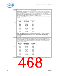
Bit
Description
63:33
Reserved.
USB6_STS — R/WC.
0 = Disable.
1 = Set by hardware and can be reset by writing a one to this bit position or a
resume well reset. This bit is set when USB UHCI controller #6 needs to cause a
wake. Additionally if the USB6_EN bit is set, the setting of the USB6_STS bit will
generate a wake event.
32
GPIOn_STS — R/WC.
0 = Software clears this bit by writing a 1 to it.
1 = These bits are set any time the corresponding GPIO is set up as an input and the
corresponding GPIO signal is high (or low if the corresponding GP_INV bit is set).
If the corresponding enable bit is set in the GPE0_EN register, then when the
GPIO[n]_STS bit is set:
31:16
• If the system is in an S1–S5 state, the event will also wake the system.
• If the system is in an S0 state (or upon waking back to an S0 state), a SCI will be
caused depending on the GPIO_ROUT bits (D31:F0:B8h, bits 31:30) for the
corresponding GPI.
NOTE: Mapping is as follows: bit 31 corresponds to GPIO[15]... and bit 16
corresponds to GPIO[0].
15
14
Reserved
USB4_STS — R/WC.
0 = Disable.
1 = Set by hardware and can be reset by writing a one to this bit position or a
resume well reset. This bit is set when USB UHCI controller #4 needs to cause a
wake. Additionally if the USB4_EN bit is set, the setting of the USB4_STS bit will
generate a wake event.
470
Datasheet

 INTEL [ INTEL ]