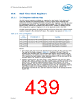
LPC Interface Bridge Registers (D31:F0)
13.6.2.2
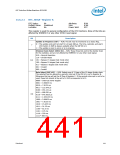
RTC_REGB—Register B (General Configuration)
RTC Index:
Default Value:
Lockable:
0Bh
U0U00UUU (U: Undefined) Size:
No Power Well:
Attribute:
R/W
8-bit
RTC
Bit
Description
Update Cycle Inhibit (SET) — R/W. Enables/Inhibits the update cycles. This bit is not
affected by RSMRST# nor any other reset signal.
0 = Update cycle occurs normally once each second.
1 = A current update cycle will abort and subsequent update cycles will not occur until
SET is returned to 0. When set is one, the BIOS may initialize time and calendar
bytes safely.
7
NOTE: This bit should be set then cleared early in BIOS POST after each powerup
directly after coin-cell battery insertion.
Periodic Interrupt Enable (PIE) — R/W. This bit is cleared by RSMRST#, but not on
any other reset.
6
5
0 = Disable.
1 = Enable. Allows an interrupt to occur with a time base set with the RS bits of register
A.
Alarm Interrupt Enable (AIE) — R/W. This bit is cleared by RTCRST#, but not on any
other reset.
0 = Disable.
1 = Enable. Allows an interrupt to occur when the AF is set by an alarm match from the
update cycle. An alarm can occur once a second, one an hour, once a day, or one a
month.
Update-Ended Interrupt Enable (UIE) — R/W. This bit is cleared by RSMRST#, but
not on any other reset.
4
3
2
0 = Disable.
1 = Enable. Allows an interrupt to occur when the update cycle ends.
Square Wave Enable (SQWE) — R/W. This bit serves no function in the ICH10. It is
left in this register bank to provide compatibility with the Motorola 146818B. The ICH10
has no SQW pin. This bit is cleared by RSMRST#, but not on any other reset.
Data Mode (DM) — R/W. This bit specifies either binary or BCD data representation.
This bit is not affected by RSMRST# nor any other reset signal.
0 = BCD
1 = Binary
Hour Format (HOURFORM) — R/W. This bit indicates the hour byte format. This bit is
not affected by RSMRST# nor any other reset signal.
1
0
0 = Twelve-hour mode. In twelve-hour mode, the seventh bit represents AM as 0 and
PM as one.
1 = Twenty-four hour mode.
Daylight Savings Legacy Software Support (DSLSWS) — R/W. Daylight savings
functionality is no longer supported. This bit is used to maintain legacy software
support and has no associated functionality. If BUC.DSO bit is set, the DSLSWS bit
continues to be R/W.
442
Datasheet

 INTEL [ INTEL ]