LPC Interface Bridge Registers (D31:F0)
13.6
Real Time Clock Registers
13.6.1
I/O Register Address Map
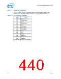
The RTC internal registers and RAM are organized as two banks of 128 bytes each,
called the standard and extended banks. The first 14 bytes of the standard bank
contain the RTC time and date information along with four registers, A–D, that are used
for configuration of the RTC. The extended bank contains a full 128 bytes of battery
backed SRAM, and will be accessible even when the RTC module is disabled (via the
RTC configuration register). Registers A–D do not physically exist in the RAM.
All data movement between the host processor and the real-time clock is done through
registers mapped to the standard I/O space. The register map appears in Table 13-6.
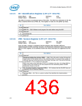
Table 13-6. RTC I/O Registers
I/O
If U128E bit = 0
Function
Locations
70h and 74h Also alias to 72h and 76h Real-Time Clock (Standard RAM) Index Register
71h and 75h Also alias to 73h and 77h Real-Time Clock (Standard RAM) Target Register
72h and 76h
73h and 77h
Extended RAM Index Register (if enabled)
Extended RAM Target Register (if enabled)
NOTES:
1. I/O locations 70h and 71h are the standard legacy location for the real-time clock.
The map for this bank is shown in Table 13-7. Locations 72h and 73h are for
accessing the extended RAM. The extended RAM bank is also accessed using an
indexed scheme. I/O address 72h is used as the address pointer and I/O address
73h is used as the data register. Index addresses above 127h are not valid. If the
extended RAM is not needed, it may be disabled.
2. Software must preserve the value of bit 7 at I/O addresses 70h and 74h. When
writing to this address, software must first read the value, and then write the same
value for bit 7 during the sequential address write. Note that port 70h is not
directly readable. The only way to read this register is through Alt Access mode.
Although RTC Index bits 6:0 are readable from port 74h, bit 7 will always return 0.
If the NMI# enable is not changed during normal operation, software can
alternatively read this bit once and then retain the value for all subsequent writes
to port 70h.
Datasheet
439

 INTEL [ INTEL ]