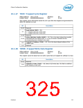
Chipset Configuration Registers
10.1.50 DMC—DMI Miscellaneous Control Register
Offset Address: 2010–2013h
Attribute:
Size:
R/W
32-bit
Default Value:
00000002h
Bit
Description
31:20
Reserved
DMI Misc. Control Field 1 — R/W. BIOS shall always program this field as per the
BIOS Specification.
19
0 = Disable DMI Power Savings.
1 = Enable DMI Power Savings.
18:0
Reserved
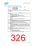
10.1.51 CIR6—Chipset Initialization Register 6
Offset Address: 2024–2027h
Attribute:
Size:
R/W
32-bit
Default Value:
0B4030C0h
Bit
Description
31:8
7
Reserved
CIR6 Field 1 — R/W. BIOS must clear this bit.
6:0
Reserved
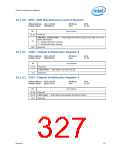
10.1.52 CIR7—Chipset Initialization Register 7
Offset Address: 2034–2037h
Attribute:
Size:
R/W
32-bit
Default Value:
B2B477CCh
Bit
Description
31:20
19:16
15:0
Reserved
CIR7 Field 1 — R/W. BIOS must program this field to 0101b.
Reserved
Datasheet
327

 INTEL [ INTEL ]