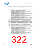
Chipset Configuration Registers
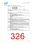
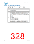
10.1.49 IOTRn — I/O Trap Register (0-3)
Offset Address: 1E80–1E87h Register 0
1E88–1E8Fh Register 1
Attribute:
R/W
1E90–1E97h Register 2
1E98–1E9Fh Register 3
Default Value:
0000000000000000h
Size:
64-bit
These registers are used to specify the set of I/O cycles to be trapped and to enable
this functionality.
Bit
Description
63:50
Reserved
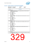
Read/Write Mask (RWM) — R/W.
49
48
0 = The cycle must match the type specified in bit 48.
1 = Trapping logic will operate on both read and write cycles.
Read/Write# (RWIO) — R/W.
0 = Write
1 = Read
NOTE: The value in this field does not matter if bit 49 is set.
47:40
39:36
Reserved
Byte Enable Mask (BEM) — R/W. A 1 in any bit position indicates that any value in
the corresponding byte enable bit in a received cycle will be treated as a match. The
corresponding bit in the Byte Enables field, below, is ignored.
35:32
31:24
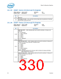
Byte Enables (TBE) — R/W. Active-high dword-aligned byte enables.
Reserved
Address[7:2] Mask (ADMA) — R/W. A 1 in any bit position indicates that any value
in the corresponding address bit in a received cycle will be treated as a match. The
corresponding bit in the Address field, below, is ignored. The mask is only provided
for the lower 6 bits of the dword address, allowing for traps on address ranges up to
256 bytes in size.
23:18
17:16
15:2
1
Reserved
I/O Address[15:2] (IOAD) — R/W. dword-aligned address
Reserved
Trap and SMI# Enable (TRSE) — R/W.
0
0 = Trapping and SMI# logic disabled.
1 = The trapping logic specified in this register is enabled.
326
Datasheet

 INTEL [ INTEL ]