Chipset Configuration Registers
Bit
Description
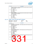
UHCI #2 Pin (U1P) — R/W. Indicates which pin the UHCI controller #2 (Device 29
Function 1) drives as its interrupt.
0h = No interrupt
1h = INTA#
7:4
2h = INTB# (Default)
3h = INTC#
4h = INTD#
5h-7h = Reserved
UHCI #1 Pin (U0P) — R/W. Indicates which pin the UHCI controller #1 (Device 29
Function 0) drives as its interrupt.
0h = No interrupt
1h = INTA# (Default)
2h = INTB#
3:0
3h = INTC#
4h = INTD#
5h-7h = Reserved
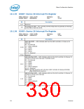
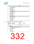
10.1.57 D28IP—Device 28 Interrupt Pin Register
Offset Address: 310C–310Fh
Attribute:
Size:
R/W
32-bit
Default Value:
00214321h
Bit
Description
31:16
23:20
Reserved
PCI Express* #6 Pin (P6IP) — R/W. Indicates which pin the PCI Express* port #6
drives as its interrupt.
0h = No interrupt
1h = INTA#
2h = INTB# (Default)
3h = INTC#
4h = INTD#
5h-7h = Reserved
PCI Express #5 Pin (P5IP) — R/W. Indicates which pin the PCI Express port #5
drives as its interrupt.
0h = No interrupt
1h = INTA# (Default)
2h = INTB#
3h = INTC#
4h = INTD#
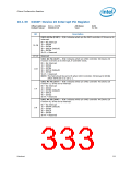
19:16
15:12
5h-7h = Reserved
PCI Express #4 Pin (P4IP) — R/W. Indicates which pin the PCI Express* port #4
drives as its interrupt.
0h = No interrupt
1h = INTA#
2h = INTB#
3h = INTC#
4h = INTD# (Default)
5h-7h = Reserved
Datasheet
331

 INTEL [ INTEL ]