Chipset Configuration Registers
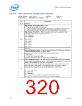
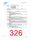
10.1.44 CIR13—Chipset Initialization Register 13
Offset Address: 0F20h–0F23h
Attribute:
Size:
R/W
32-bit
Default Value:
B2B477CCh
Bit
Description
31:20
19:16
15:0
Reserved
CIR13 Field 1 — R/W. BIOS must program this field to 0101b.
Reserved
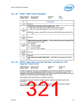
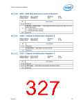
10.1.45 CIR5—Chipset Initialization Register 5
Offset Address: 1D40h–1D47h
Attribute:
Size:
R/W
64-bit
Default Value:
0000000000000000h
Bit
Description
63:1
0
Reserved
CIR5 Field 1 — R/W. BIOS must program this field to 1b.
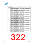
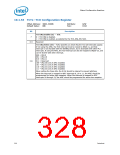
10.1.46 TRSR—Trap Status Register
Offset Address: 1E00–1E03h
Attribute:
Size:
R/WC, RO
32-bit
Default Value:
00000000h
Bit
Description
31:4
3:0
Reserved
Cycle Trap SMI# Status (CTSS) — R/WC. These bits are set by hardware when the
corresponding Cycle Trap register is enabled and a matching cycle is received (and
trapped). These bits are OR’ed together to create a single status bit in the Power
Management register space.
Note that the SMI# and trapping must be enabled in order to set these bits.
These bits are set before the completion is generated for the trapped cycle, thereby
ensuring that the processor can enter the SMI# handler when the instruction
completes. Each status bit is cleared by writing a 1 to the corresponding bit location
in this register.
324
Datasheet

 INTEL [ INTEL ]