Electrical Characteristics
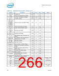
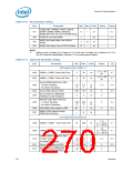
Table 8-10. PCI Interface Timing
Sym
Parameter
Min Max Units
Notes
Figure
C/BE[3:0]#, FRAME#, TRDY#, IRDY#,
STOP#, SERR#, PERR#, DEVSEL#,
REQ[A:B]# Hold Time from PCLKIN Rising
t47
0
—
ns
8-3
8-5
t48
t49
t50
PCIRST# Low Pulse Width
1
2
ms
ns
ns
GNT[3:0]# Valid Delay from PCICLK
Rising
12
—
REQ[3:0]# Setup Time to PCICLK Rising
12
NOTE:
1.
Refer to note 3 of table 4-4 in Section 4.2.2.2 and note 2 of table 4-6 in Section 4.2.3.2 of
the PCI Local Bus Specification, Revision 2.3 for measurement details.
Table 8-11. Universal Serial Bus Timing
Sym
Parameter
Min
Max
Units
Notes
Fig
Full-speed Source (Note 7)
1, C = 50
L
t100
t101
USBPx+, USBPx- Driver Rise Time
USBPx+, USBPx- Driver Fall Time
4
4
20
20
ns
ns
8-7
8-7
pF
1, C = 50
L
pF
Source Differential Driver Jitter
- To Next Transition
t102
–3.5
–4
3.5
4
ns
ns
2, 3
8-8
8-9
- For Paired Transitions
t103
t104
Source SE0 interval of EOP
160
–2
175
5
ns
ns
4
5
Source Jitter for Differential
Transition to SE0 Transition
Receiver Data Jitter Tolerance
- T o Next Transition
t105
–18.5 18.5
ns
ns
3
4
8-8
8-9
–9
9
- For Paired Transitions
t106
t107
EOP Width: Must accept as EOP
82
—
ns
ns
Width of SE0 interval during
differential transition
—
14
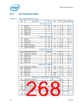
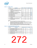
Low-speed Source (Note 8)
1, 6
t108
t109
USBPx+, USBPx – Driver Rise Time
USBPx+, USBPx – Driver Fall Time
75
75
300
300
ns
ns
C = 50 pF
C = 350 pF
L
8-7
8-7
L
1,6
C = 50 pF
L
C = 350 pF
L
Source Differential Driver Jitter
To Next Transition
t110
–25
–14
25
14
ns
ns
2, 3
8-8
8-9
For Paired Transitions
t111
t112
Source SE0 interval of EOP
1.25
–40
1.50
100
µs
ns
4
5
Source Jitter for Differential
Transition to SE0 Transition
270
Datasheet

 INTEL [ INTEL ]