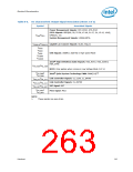
Electrical Characteristics
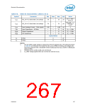
Table 8-8.
Symbol
Other DC Characteristics (Sheet 2 of 2)
Parameter
Min
Nom
Max
Unit
Notes
(0 V < VIN <
Vcc3_3)
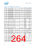
I
PCI_3V Hi-Z State Data Line Leakage
–10
—
10
µA
LI2
Max V = 2.7
IN
I
I
PCI_5V Hi-Z State Data Line Leakage
–70
—
70
µA
V Min V
=
IN
LI3
LI4
0.5 V
Input Leakage Current – Clock signals
Input Capacitance – All Other
Output Capacitance
–100
—
—
—
—
—
+100
12
µA
pF
pF
pF
2
C
F
C
F
C
F
C
= 1 MHz
= 1 MHz
= 1 MHz
IN
C
—
12
OUT
C
I/O Capacitance
—
12
I/O
Typical Value
C
C
XTAL1
XTAL2
6
6
pF
pF
L
L
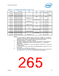
NOTES:
1.
The I/O buffer supply voltage is measured at the ICH package pins. The tolerances shown
in Table 8-8 are inclusive of all noise from DC up to 20 MHz. In testing, the voltage rails
should be measured with a bandwidth limited oscilloscope that has a rolloff of 3 dB/decade
above 20 MHz.
2.
3.
Includes CLK14, CLK48, GLAN_CLK and PCICLK
CL_VREF voltage applies when pin is driven by external circuit.
Datasheet
267

 INTEL [ INTEL ]