Functional Description
5.23.8
Serial Flash Device Package
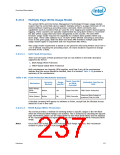
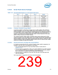
Table 5-62. Recommended Pinout for 16-Pin Serial Flash Device
Pin #
Signal
Pin #
Signal
1
2
3
4
5
6
7
8
Hold / Reset
Supply Voltage
No Connect
9
Write Protect
Ground
10
11
12
13
14
15
16
No Connect
No Connect
No Connect
No Connect
Serial Data In
Serial Clock
No Connect
No Connect
No Connect
Chip Select
Serial Data Out
5.23.8.1
Common Footprint Usage Model
To minimize platform motherboard redesign and to enable platform Bill of Material
(BOM) selectability, many PC System OEM’s design their motherboard with a single
common footprint. This common footprint allows population of a soldered down device
or a socket that accepts a leadless device. This enables the board manufacturer to
support, via selection of the appropriate BOM, either of these solutions on the same
system without requiring any board redesign.
The common footprint usage model is desirable during system debug and by flash
content developers since the leadless device can be easily removed and reprogrammed
without damage to device leads. When the board and flash content is mature for high-
volume production, both the socketed leadless solution and the soldered down leaded
solution are available through BOM selection.
5.23.8.2
Serial Flash Device Package Recommendations
It is highly recommended that the common footprint usage model be supported. An
example of how this can be accomplished is as follows:
• The recommended pinout for 8-pin serial flash devices is used (refer to
Section 5.23.7).
• The 8-pin device is supported in either an 8-contact VDFPN (6x5 mm MLP) package
or an 8-contact WSON (5x6 mm) package. These packages can fit into a socket
that is land pattern compatible with the wide body SO8 package.
• The 8-pin device is supported in the SO8 (150 mil) and in the wide-body SO8
(200 mil) packages.
The 16-pin device is supported in the SO16 (300 mil) package.
Datasheet
239

 INTEL [ INTEL ]