Functional Description
5.23.4.3.1
SPI Flash Unlocking Requirements for Intel Management Engine
Flash devices must be globally unlocked (read, write and erase access on the Intel ME
region) from power on by writing 00h to the flash’s status register to disable write
protection.
If the status register must be unprotected, it must use the enable write status register
command 50h or write enable 06h.
Opcode 01h (write to status register) must then be used to write a single byte of 00h
into the status register. This must unlock the entire part. If the SPI flash’s status
register has non-volatile bits that must be written to, bits [5:2] of the flash’s status
register must be all 0h to indicate that the flash is unlocked.
If there is no need to execute a write enable on the status register, then opcodes 06h
and 50h must be ignored.
After global unlock, BIOS has the ability to lock down small sections of the flash as long
as they do not involve the Intel ME or GbE region.
5.23.4.4
Hardware Sequencing Requirements
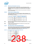
Table 5-59 contains a list of commands and the associated opcodes that a SPI-based
serial flash device must support in order to be compatible with hardware sequencing.
Table 5-59. Hardware Sequencing Commands and Opcode Requirements
Commands
Opcode
Notes
Writes a byte to SPI flash’s status register. Enable Write
to Status Register command must be run prior to this
command.
Write to Status Register
01h
Single byte or 64 byte write as determined by flash part
capabilities and software.
Program Data
02h
Read Data
03h
04h
05h
06h
0Bh
Write Disable
Read Status
Write Enable
Fast Read
Outputs contents of SPI flash’s status register
Enable Write to Status
Register
50h or
60h
Enables a bit in the status register to allow an update to
the status register
Program
mable
Erase
256B, 4 Kbyte, 8 Kbyte or 64 Kbyte
Full Chip Erase
JEDEC ID
C7h
9Fh
See Section .
5.23.4.4.1
JEDEC ID
Since each serial flash device may have unique capabilities and commands, the JEDEC
ID is the necessary mechanism for identifying the device so the uniqueness of the
device can be comprehended by the controller (master). The JEDEC ID uses the opcode
9Fh and a specified implementation and usage model. This JEDEC Standard
Manufacturer and Device ID read method is defined in Standard JESD21-C, PRN03-NV.
236
Datasheet

 INTEL [ INTEL ]