Functional Description
5.23.5.3
SMI# Based Global Write Protection
The ICH provides a method for blocking writes to the SPI flash when the Write
Protected bit is cleared (i.e., protected). This is achieved by checking the Opcode type
information (which can be locked down by the initial Boot BIOS) of the requested
command.
The Write Protect and Lock Enable bits interact in the same manner for SPI BIOS as
they do for the FWH BIOS.
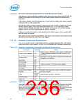
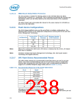
5.23.6
Flash Device Configurations
The ICH10-based platform may use the serial flash in multiple configurations. The
following table focuses on the supported configurations involving the ICH10 and Intel
Active Management Technology.
System BIOS
Storage
Intel®ICH10
Firmware
Minimum Number
of SPI Device(s)
Configuration
1
2
3
4
SPI
No
Yes
Yes
No
1
1
1
0
Non-SPI
SPI
Non-SPI
Note:
Note:
When SPI is selected for BIOS and a SPI device is detected by the ICH10, LPC based
BIOS flash is disabled.
Firmware includes Intel Active Management Technology, ASF, Intel Quiet System
Technology and Gigabit Ethernet.
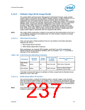
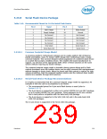
5.23.7
SPI Flash Device Recommended Pinout
The table below contains the recommended serial flash device pin-out for an 8-pin
device. Use of the recommended pin-out on an 8-pin device reduces complexities
involved with designing the serial flash device onto a motherboard and allows for
support of a common footprint usage model (refer to Section 5.23.8.1).
Table 5-61. Recommended Pinout for 8-Pin Serial Flash Device
Pin #
Signal
1
2
3
4
5
6
7
8
Chips Select
Data Output
Write Protect
Ground
Data Input
Serial Clock
Hold / Reset
Supply Voltage
Although an 8-pin device is preferred over a 16-pin device due to footprint
compatibility, the following table contains the recommended serial flash device pin-out
for a 16-pin SOIC.
238
Datasheet

 INTEL [ INTEL ]