Functional Description
5.23.5
Multiple Page Write Usage Model
The system BIOS and Intel Active Management Technology firmware usage models
require that the serial flash device support multiple writes to a page (minimum of 512
writes) without requiring a preceding erase command. BIOS commonly uses
capabilities such as counters that are used for error logging and system boot progress
logging. These counters are typically implemented by using byte-writes to ‘increment’
the bits within a page that have been designated as the counter. The Intel AMT
firmware usage model requires the capability for multiple data updates within any
given page. These data updates occur via byte-writes without executing a preceding
erase to the given page. Both the BIOS and Intel AMT firmware multiple page write
usage models apply to sequential and non-sequential data writes.
Note:
This usage model requirement is based on any given bit only being written once from a
1-to-0 without requiring the preceding erase. An erase would be required to change
bits back to the 1 state.
5.23.5.1
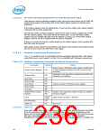
Soft Flash Protection
There are two types of flash protection that are not defined in the flash descriptor
supported by ICH10:
1. BIOS Range Write Protection
2. SMI#-Based Global Write Protection
Both mechanisms are logically OR’d together such that if any of the mechanisms
indicate that the access should be blocked, then it is blocked. Table 5-60 provides a
summary of the mechanisms.
Table 5-60. Flash Protection Mechanism Summary
Reset-Override
or SMI#-
Accesses
Blocked
Range
Specific?
Equivalent Function on
FWH
Mechanism
Override?
BIOS Range
Write
Protection
Writes
Yes
No
Reset Override
SMI# Override
FWH Sector Protection
Same as Write Protect in
previous ICHs for FWH
Write Protect
Writes
A blocked command will appear to software to finish, except that the Blocked Access
status bit is set in this case.
5.23.5.2
BIOS Range Write Protection
The ICH10 provides a method for blocking writes to specific ranges in the SPI flash
when the Protected BIOS Ranges are enabled. This is achieved by checking the Opcode
type information (which can be locked down by the initial Boot BIOS) and the address
of the requested command against the base and limit fields of a Write Protected BIOS
range.
Note:
Once BIOS has locked down the Protected BIOS Range registers, this mechanism
remains in place until the next system reset.
Datasheet
237

 INTEL [ INTEL ]