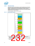
Functional Description
3. The component section has information about the SPI flash in the system including:
the number of components, density of each, invalid instructions (such as chip
erase), and frequencies for read, fast read and write/erase instructions.
4. The Region section points to the three other regions as well as the size of each
region.
5. The master region contains the security settings for the flash, granting read/write
permissions for each region and identifying each master by a requestor ID. See
Section 5.23.2.1 for more information.
6 & 7. The (G)MCH and ICH chipset soft strap sections contain (G)MCH and ICH
configurable parameters.
8. The Reserved region between the top of the (G)MCH strap section and the bottom of
the OEM Section is reserved for future chipset usages.
9. The Descriptor Upper MAP determines the length and base address of the Intel
Management Engine VSCC Table.
10. The Intel Management Engine VSCC Table holds the JEDEC ID and the VSCC
information of the entire SPI Flash supported by the NVM image.
11. OEM Section is 256 Bytes reserved at the top of the Flash Descriptor for use by
OEM.
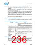
5.23.2.1
Descriptor Master Region
The master region defines read and write access setting for each region of the SPI
device. The master region recognizes three masters: BIOS, Gigabit Ethernet, and Intel
Management Engine. Each master is only allowed to do direct reads of its primary
regions.
Table 5-58. Region Access Control Table
Master Read/Write Access
Region
CPU and BIOS
Intel ME/(G)MCH
N/A
GbE Controller
Descriptor
N/A
N/A
CPU and BIOS can
always read from and
write to BIOS Region
BIOS
Read / Write
Read / Write
Read / Write
Intel ME can always
read from and write to
Intel ME Region
Intel Management
Engine
Read / Write
GbE software can
always read from and
write to GbE region
Gigabit Ethernet
Read / Write
N/A
Read / Write
N/A
Platform Data Region
N/A
Datasheet
233

 INTEL [ INTEL ]