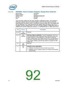
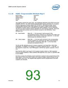
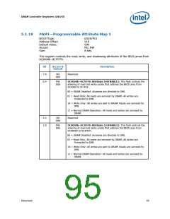
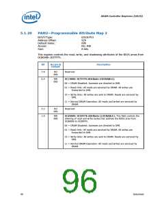
DRAM Controller Registers (D0:F0)
5.1.20
PAM2—Programmable Attribute Map 2
B/D/F/Type:
Address Offset:
Default Value:
Access:
0/0/0/PCI
92h
00h
RO, RW
8 bits
Size:
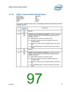
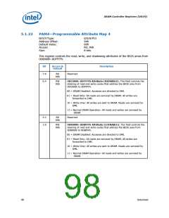
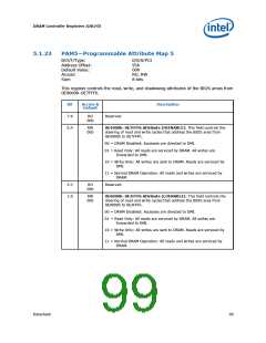
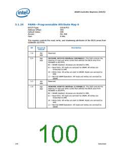
This register controls the read, write, and shadowing attributes of the BIOS areas from
0C8000h–0CFFFFh.
Bit
7:6
5:4
Access &
Default
Description
RO
00b
Reserved
RW
0CC000h–0CFFFFh Attribute (HIENABLE):
00b
00 = DRAM Disabled: Accesses are directed to DMI.
01 = Read Only: All reads are serviced by DRAM. All writes are
forwarded to DMI.
10 = Write Only: All writes are sent to DRAM. Reads are serviced by
DMI.
11 = Normal DRAM Operation: All reads and writes are serviced by
DRAM.
3:2
1:0
RO
00b
Reserved
RW
00b
0C8000h–0CBFFFh Attribute (LOENABLE): This field controls the
steering of read and write cycles that address the BIOS area from
0C8000h to 0CBFFFh.
00 = DRAM Disabled: Accesses are directed to DMI.
01 = Read Only: All reads are serviced by DRAM. All writes are
forwarded to DMI.
10 = Write Only: All writes are sent to DRAM. Reads are serviced by
DMI.
11 = Normal DRAM Operation: All reads and writes are serviced by
DRAM.
96
Datasheet

 INTEL [ INTEL ]