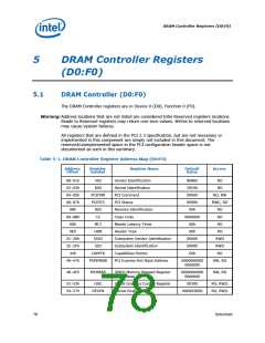
DRAM Controller Registers (D0:F0)
5 DRAM Controller Registers
(D0:F0)
5.1
DRAM Controller (D0:F0)
The DRAM Controller registers are in Device 0 (D0), Function 0 (F0).
Warning:Address locations that are not listed are considered Intel Reserved registers locations.
Reads to Reserved registers may return non-zero values. Writes to reserved locations
may cause system failures.
All registers that are defined in the PCI 2.3 specification, but are not necessary or
implemented in this component are simply not included in this document. The
reserved/unimplemented space in the PCI configuration header space is not
documented as such in this summary.
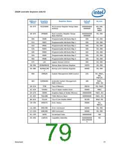
Table 5-1. DRAM Controller Register Address Map (D0:F0)
Address
Offset
Register
Symbol
Register Name
Default
Value
Access
00–01h
02–03h
04–05h
06–07h
08h
VID
DID
Vendor Identification
8086h
29C0h
0006h
0090h
00h
RO
RO
Device Identification
PCI Command
PCICMD
PCISTS
RID
RO, RW
RWC, RO
RO
PCI Status
Revision Identification
Class Code
09–0Bh
0Dh
CC
060000h
00h
RO
MLT
Master Latency Timer
Header Type
RO
0Eh
HDR
00h
RO
2C–2Dh
2E–2Fh
34h
SVID
Subsystem Vendor Identification
Subsystem Identification
Capabilities Pointer
PCI Express Port Base Address
0000h
0000h
E0h
RWO
RWO
RO
SID
CAPPTR
PXPEPBAR
40–47h
0000000000
000000h
RW, RO
48–4Fh
MCHBAR
GMCH Memory Mapped Register
Range Base
0000000000
000000h
RW, RO
52–53h
54–57h
GGC
GMCH Graphics Control Register
Device Enable
0030h
RO, RW/L
RO, RW/L
DEVEN
000003DBh
78
Datasheet

 INTEL [ INTEL ]