System Address Map
3.8.1
SMM Space Definition
SMM space is defined by its addressed SMM space and its DRAM SMM space. The
addressed SMM space is defined as the range of bus addresses used by the processor
to access SMM space. DRAM SMM space is defined as the range of physical DRAM
memory locations containing the SMM code. SMM space can be accessed at one of
three transaction address ranges: Compatible, High and TSEG. The Compatible and
TSEG SMM space is not remapped and therefore the addressed and DRAM SMM space
is the same address range. Since the High SMM space is remapped the addressed and
DRAM SMM space is a different address range. Note that the High DRAM space is the
same as the Compatible Transaction Address space. Table 3-6 describes three unique
address ranges.
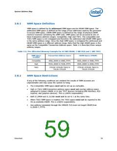
Table 3-6. Pre-Allocated Memory Example for 64-MB DRAM, 1-MB VGA and 1-MB TSEG
SMM Space
Enabled
Transaction Address Space
DRAM Space (DRAM)
Compatible
High
000A_0000h to 000B_FFFFh
FEDA_0000h to FEDB_FFFFh
000A_0000h to 000B_FFFFh
000A_0000h to 000B_FFFFh
TSEG
(TOLUD–STOLEN–TSEG) to
TOLUD–STOLEN
(TOLUD–STOLEN–TSEG) to
TOLUD–STOLEN
3.8.2
SMM Space Restrictions
If any of the following conditions are violated the results of SMM accesses are
unpredictable and may cause the system to hang:
•
•
The Compatible SMM space must not be set-up as cacheable.
High or TSEG SMM transaction address space must not overlap address space
assigned to system DRAM, or to any “PCI” devices (including DMI Interface, PCI-
Express, and graphics devices). This is a BIOS responsibility.
•
•
Both D_OPEN and D_CLOSE must not be set to 1 at the same time.
When TSEG SMM space is enabled, the TSEG space must not be reported to the
OS as available DRAM. This is a BIOS responsibility.
•
Any address translated through the GMADR TLB must not target DRAM from
A_0000-F_FFFFh.
Datasheet
59

 INTEL [ INTEL ]