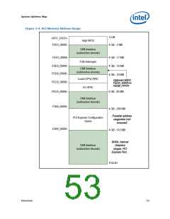
System Address Map
3.6
PCI Express* Graphics Attach (PEG)
The GMCH can be programmed to direct memory accesses to the PCI Express
interface when addresses are within either of two ranges specified via registers in
GMCH’s Device 1 configuration space.
•
The first range is controlled via the Memory Base Register (MBASE) and Memory
Limit Register (MLIMIT) registers.
•
The second range is controlled via the Pre-fetchable Memory Base (PMBASE) and
Pre-fetchable Memory Limit (PMLIMIT) registers.
Conceptually, address decoding for each range follows the same basic concept. The
top 12 bits of the respective Memory Base and Memory Limit registers correspond to
address bits A[31:20] of a memory address . For the purpose of address decoding, the
GMCH assumes that address bits A[19:0] of the memory base are zero and that
address bits A[19:0] of the memory limit address are FFFFFh. This forces each
memory address range to be aligned to 1MB boundary and to have a size granularity
of 1 MB.
The GMCH positively decodes memory accesses to PCI Express memory address space
as defined by the following equations:
Memory_Base_Address ≤ Address ≤ Memory_Limit_Address
Prefetchable_Memory_Base_Address ≤ Address ≤ Prefetchable_Memory_Limit_Address
The window size is programmed by the plug-and-play configuration software. The
window size depends on the size of memory claimed by the PCI Express device.
Normally these ranges will reside above the Top-of-Low Usable-DRAM and below High
BIOS and APIC address ranges. They MUST reside above the top of low memory
(TOLUD) if they reside below 4 GB and MUST reside above top of upper memory
(TOUUD) if they reside above 4 GB or they will steal physical DRAM memory space.
It is essential to support a separate Pre-fetchable range in order to apply USWC
attribute (from the processor point of view ) to that range. The USWC attribute is used
by the processor for write combining.
Note that the GMCH Device 1 memory range registers described above are used to
allocate memory address space for any PCI Express devices sitting on PCI Express
that require such a window.
The PCICMD1 register can override the routing of memory accesses to PCI Express. In
other words, the memory access enable bit must be set in the device 1 PCICMD1
register to enable the memory base/limit and pre-fetchable base/limit windows.
The upper PMUBASE1/PMULIMIT1 registers have been implemented for PCI Express
Specification compliance. The GMCH 36 bit addressing locates MMIO space above 4 GB
using these registers.
Datasheet
57

 INTEL [ INTEL ]