System Address Map
3.3.1
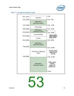
APIC Configuration Space (FEC0_0000h–FECF_FFFFh)
This range is reserved for APIC configuration space. The I/O APIC(s) usually reside in
the ICH portion of the chipset, but may also exist as stand-alone components like
PXH.
The IOAPIC spaces are used to communicate with IOAPIC interrupt controllers that
may be populated in the system. Since it is difficult to relocate an interrupt controller
using plug-and-play software, fixed address decode regions have been allocated for
them. Processor accesses to the default IOAPIC region (FEC0_0000h to FEC7_FFFFh)
are always forwarded to DMI.
The GMCH optionally supports additional I/O APICs behind the PCI Express “Graphics”
port. When enabled via the PCI Express Configuration register (Device 1 Offset 200h),
the PCI Express port will positively decode a subset of the APIC configuration space –
specifically FEC8_0000h thru FECF_FFFFh. Memory request to this range would then
be forwarded to the PCI Express port. This mode is intended for the entry
Workstation/Server SKU of the GMCH, and would be disabled in typical Desktop
systems. When disabled, any access within entire APIC Configuration space
(FEC0_0000h to FECF_FFFFh) is forwarded to DMI.
3.3.2
HSEG (FEDA_0000h–FEDB_FFFFh)
This optional segment from FEDA_0000h to FEDB_FFFFh provides a remapping
window to SMM Memory. It is sometimes called the High SMM memory space. SMM-
mode processor accesses to the optionally enabled HSEG are remapped to 000A-
_0000h – 000B_FFFFh. Non-SMM-mode processor accesses to enabled HSEG are
considered invalid and are terminated immediately on the FSB. The exceptions to this
rule are Non-SMM-mode Write Back cycles which are remapped to SMM space to
maintain cache coherency. PCI Express and DMI originated cycles to enabled SMM
space are not allowed. Physical DRAM behind the HSEG transaction address is not
remapped and is not accessible. All Cacheline writes with WB attribute or Implicit
write backs to the HSEG range are completed to DRAM like an SMM cycle.
3.3.3
3.3.4
FSB Interrupt Memory Space (FEE0_0000–FEEF_FFFFh)
The FSB Interrupt space is the address used to deliver interrupts to the FSB. Any
device on PCI Express or DMI may issue a Memory Write to 0FEEx_xxxxh. The GMCH
will forward this Memory Write along with the data to the FSB as an Interrupt Message
Transaction. The GMCH terminates the FSB transaction by providing the response and
asserting HTRDY#. This Memory Write cycle does not go to DRAM.
High BIOS Area
The top 2 MB (FFE0_0000h -FFFF_FFFFh) of the PCI Memory Address Range is
reserved for System BIOS (High BIOS), extended BIOS for PCI devices, and the A20
alias of the system BIOS. The processor begins execution from the High BIOS after
reset. This region is mapped to DMI Interface so that the upper subset of this region
aliases to 16 MB-256 KB range. The actual address space required for the BIOS is less
than 2 MB but the minimum processor MTRR range for this region is 2 MB so that full
2 MB must be considered.
54
Datasheet

 INTEL [ INTEL ]