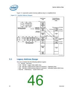
System Address Map
3.1.6
PAM Memory Area Details
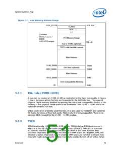
The 13 sections from 768 KB to 1 MB comprise what is also known as the PAM
Memory Area.
The GMCH does not handle IWB (Implicit Write-Back) cycles targeting DMI. Since all
memory residing on DMI should be set as non-cacheable, there will normally not be
IWB cycles targeting DMI.
However, DMI becomes the default target for processor and DMI originated accesses
to disabled segments of the PAM region. If the MTRRs covering the PAM regions are
set to WB or RD it is possible to get IWB cycles targeting DMI. This may occur for
processor originated cycles (in a DP system) and for DMI originated cycles to disabled
PAM regions.
For example, say that a particular PAM region is set for “Read Disabled” and the MTRR
associated with this region is set to WB. A DMI master generates a memory read
targeting the PAM region. A snoop is generated on the FSB and the result is an IWB.
Since the PAM region is “Read Disabled” the default target for the Memory Read
becomes DMI. The IWB associated with this cycle will cause the GMCH to hang.
3.1.7
Legacy Interrupt Routing
Table 3-4. Specifics of Legacy Interrupt Routing
Interrupt Source
Default Interrupt A/B/C/D
Internal Graphics D2 F0
A
PEG (External Graphics Device)
Function of what is defined in Interrupt Pin
register of the PEG device
PEG (Internally generated
Interrupt) D1 F0
A
ME (IDER) D3 F2
ME (HECI) D3 F0
ME (KT) D3 F3
B
C
A
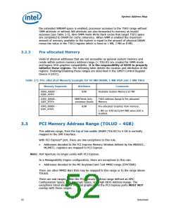
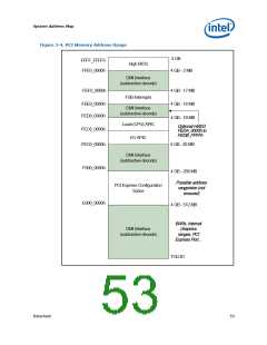
3.2
Main Memory Address Range (1MB – TOLUD)
This address range extends from 1 MB to the top of Low Usable physical memory that
is permitted to be accessible by the GMCH (as programmed in the TOLUD register). All
accesses to addresses within this range will be forwarded by the GMCH to the DRAM
unless it falls into the optional TSEG, optional ISA Hole, or optional IGD stolen VGA
memory.
50
Datasheet

 INTEL [ INTEL ]