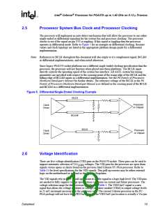
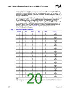
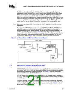
Intel® Celeron® Processor for PGA370 up to 1.40 GHz on 0.13 µ Process
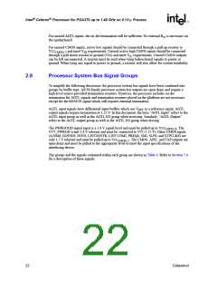
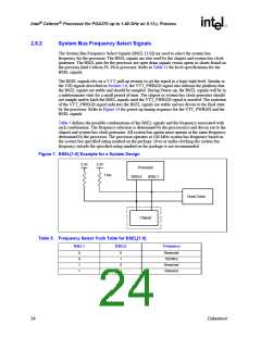
Table 4. System Bus Signal Groups 1
Group Name
Signals
AGTL Input
BPRI#, DEFER#, RESET#, RSP#
PRDY#
AGTL Output
A[35:3]#, ADS#, AERR#, AP[1:0]#, BERR#, BINIT#, BNR#, BP[3:2]#, BPM[1:0]#,
2
AGTL I/O
BR0# , D[63:0]#, DBSY#, DEP[7:0]#, DRDY#, HIT#, HITM#, LOCK#, REQ[4:0]#, RP#,
RS[2:0]#, TRDY#
CMOS Input
(1.25 V)
VTT_PWRGD
3
CMOS Input
(1.5 V)
A20M#, FLUSH#, IGNNE#, INIT#, LINT0/INTR, LINT1/NMI, PREQ#, SLP#, SMI#,
STPCLK#
4
CMOS Input
(1.8 V)
PWRGOOD
5
CMOS Output
FERR#, IERR#, THERMTRIP#
4
(1.5 V)
8
CMOS Output
VID[3:0,25mV], BSEL[1:0]
BCLK0, BCLK0#
(3.3 V)
System Bus
10
Clock
(1.25 V/2.5 V)
9
APIC Clock
PICCLK
4
APIC I/O
PICD[1:0]
4
TAP Input
TCK, TDI, TMS, TRST#
TDO
4
TAP Output
7
CPUPRES#, DYN_OE, NCHTRL, PLL[2:1], SLEWCTRL, RTTCTRL ,THERMDN,
6
Power/Other
THERMDP, VCC
, V
, VSS, VTT, Reserved,
CORE
REF
NOTES:
1. See Section 7.0 for information on the these signals.
2. The BR0# pin is the only BREQ# signal that is bidirectional. See Section 7.0 for more information.
3. This signal is 1.25 V.
4. These signals are 1.5 V.
5. This signal is 1.8 V.
6. VCC
is the power supply for the processor core and is described in Section 2.6.
CORE
VID[3:0,25mV] is described in Section 2.6.
VTT is used to terminate the system bus and generate V
VSS is system ground.
on the motherboard.
REF
BSEL[1:0] is described in Section 2.8.2 and Section 7.0.
All other signals are described in Section 7.0.
7. This signal is used to control the value of the processor on-die termination resistance. Refer to the platform
design guide for the recommended pulldown resistor value.
8. These signals are 3.3 V.
9. These signals are 2.0 V.
10. 1.25 V signal for Differential clock application and 2.5 V for Single-ended clock application.
2.8.1
Asynchronous vs. Synchronous for System Bus Signals
All AGTL signals are synchronous to BCLK (BCLK/BCLK#). All of the CMOS, Clock, APIC,
and TAP signals can be applied asynchronously to BCLK (BCLK/BCLK#). All APIC signals are
synchronous to PICCLK. All TAP signals are synchronous to TCK.
Datasheet
23

 INTEL [ INTEL ]