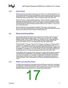
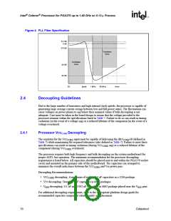
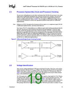
Intel® Celeron® Processor for PGA370 up to 1.40 GHz on 0.13 µ Process
The VID pins should be pulled up to a 3.3 V level. This may be accomplished with pull-ups
internal to the voltage regulator, which ensures valid VID pull-up voltage during Power-up and
Power-down sequences. If external resistors are used for the VID[3:0, 25mV] signal, then the
power source must be guaranteed to be stable whenever the supply to the voltage regulator is
stable. This will prevent the possibility of the processor supply going above the specified VCC
in the event of a failure in the supply for the VID lines. In the case of a DC-to-DC converter, CthOiRsE
can be accomplished by using the input voltage to the converter for the VID line pull-ups. A
resistor equal to 1 kΩ may be used to connect the VID signals to the voltage regulator input.
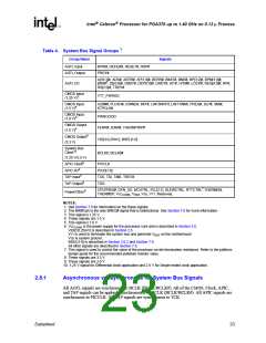
Note: Intel requires that designs utilize VRM 8.5 and Not VRM 8.4 guidelines to meet the processor
requirements.
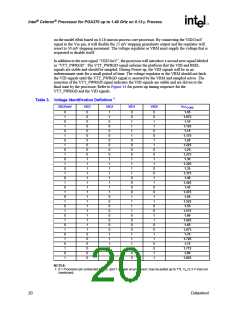
To re-emphasize, VRM 8.5 introduces two new signals [VID25mV and VTT_PWRGD] that is
utilized by the processor and platform. Ignoring and not connecting these two new pins, as
documented in the Platform Design Guidelines, will prevent the processor from operating at the
specified voltage levels and core frequency. Figure 6 provides a high-level interconnection
schematic. Refer to the VRM 8.5 DC-DC Converter Design Guideline and the appropriate Platform
Design Guidelines for further detailed information on the voltage identification and bus select
implementation. Refer to Figure 14 for VID power-up sequence and timing requirements.
Figure 6. VTT Power Good and Bus Select Interconnect Diagram
VID[3:0, 25mV]
VTT
VTT
Intel® Celeron
Processor based on
0.13 Micron Process
VRM 8.5
Voltage Regulator
VTT
1 kΩ
VCC
VCC
CORE
CORE
VTT_PWRGD
(output)
VTT_PWRGD
(input)
BSEL[1:0]
Clock
Driver
2.7
Processor System Bus Unused Pins
All RESERVED pins must remain unconnected unless specifically noted. Connection of these pins
to VCCCORE, VREF, VSS, VTT or to any other signal (including each other) can result in component
malfunction or incompatibility with future processors. See Section 5.4 for a pin listing of the
processor and the location of each RESERVED pin.
PICCLK must be driven with a valid clock input and the PICD[1:0] signals must be pulled-up to
VCCCMOS1.5 even when the APIC will not be used. A separate pull-up resistor must be provided for
each PICD signal.
For reliable operation, always connect unused inputs or bidirectional signals to their deasserted
signal level. The pull-up or pull-down resistor values are system dependent and should be chosen
such that the logic high (VIH) and logic low (VIL) requirements are met. See Table 11 for level
specifications of non-AGTL signals.
Datasheet
21

 INTEL [ INTEL ]