Intel® Celeron® Processor for PGA370 up to 1.40 GHz on 0.13 µ Process
2.8.2
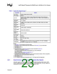
System Bus Frequency Select Signals
The System Bus Frequency Select Signals (BSEL [1:0]) are used to select the system bus
frequency for the processor. The BSEL signals are also used by the chipset and system bus clock
generator. The BSEL pins for the processor are open drain signals versus opens or shorts found on
the previous Intel Celeron FC-PGA processor. Refer to Table 11 for level specifications for the
BSEL signals.
The BSEL signals rely on a 3.3 V pull-up resistor to set the signal to a logic high level. Similar to
the VID signals described in Section 2.6, the VTT_PWRGD signal also informs the platform that
the BSEL signals are stable and should be sampled. During Power-up, the BSEL signals will be in
a indeterminate state for a small period of time. The chipset or system bus clock generator should
not sample and/or latch the BSEL signals until the VTT_PWRGD signal is asserted. The assertion
of the VTT_PWRGD signal indicates the BSEL signals are stable and are driven to the final state
by the processor. Refer to Figure 14 for power-up timing sequence for the VTT_PWRGD and the
BSEL signals.
Table 5 defines the possible combinations of the BSEL signals and the frequency associated with
each combination. The frequency selection is determined by the processor(s) and driven out to the
chipset and system bus clock generator. All system bus agents must operate at the same frequency
determined by the processor. The processor operates at 100 MHz system bus frequency based on
the system bus specified rating marked on the package. Over or under-clocking the system bus
frequency outside the specified rating marked on the package is not recommended.
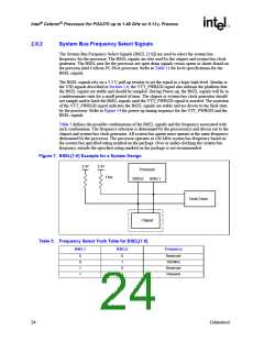
Figure 7. BSEL[1:0] Example for a System Design
3.3V
3.3V
Processor
BSEL0 BSEL1
1 kΩ
Clock Driver
Chipset
Table 5. Frequency Select Truth Table for BSEL[1:0]
BSEL1
BSEL0
Frequency
0
0
1
1
0
1
0
1
Reserved
100 MHz
Reserved
Reseved
24
Datasheet

 INTEL [ INTEL ]