Intel® Celeron® Processor for PGA370 up to 1.40 GHz on 0.13 µ Process
2.5
Processor System Bus Clock and Processor Clocking
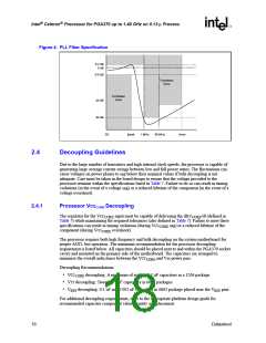
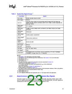
The processor will implement an auto-detect mechanism that will allow the processor to use either
single-ended or differential signaling for the system bus and processor clocking. The processor
checks to see if the signal on pin Y33 is toggling. If this signal is toggling then the processor
operates in differential mode. Refer to Figure 5 for an example on differential clocking. Resistor
values and clock topology are listed in the appropriate platform design guide for a differential
implementation.
Note: References to BCLK throughout this document will also imply to it’s complement signal, BCLK#
in differential implementations, and when noted otherwise.
Since legacy PGA370 socket platforms use a different single-ended clocking specification than the
processor, the processor will not function when placed into these platforms. The BCLK input
directly controls the operating speed of the system bus interface. All AGTL system bus timing
parameters are specified with respect to the crossing point of the rising edge of the BCLK and the
falling edge of BCLK# inputs in a differential implementation. See the P6 Family of Processors
Hardware Developer's Manual for further details. The reference voltage of the BCLK in the P6
Family of Processors Hardware Developer Manual is re-defined as the crossing point of the BCLK
and BCLK# in a differential implementation.
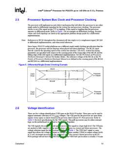
Figure 5. Differential/Single-Ended Clocking Example
BCLK
+
Processor
or Chipset
Clock
Driver
–
BCLK#
BCLK
Processor
or Chipset
Clock
Driver
2.6
Voltage Identification
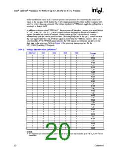
There are five voltage identification (VID) pins on the PGA370 socket. These pins can be used to
support automatic selection of VCCCORE voltages. The VID pins for the processor are open drain
signals versus opens or shorts found on the previous Intel Celeron FC-PGA processor. Refer to
Table 11 for level specifications for the VID signals. This pull-up resistor may be either external
logic on the motherboard or internal to the Voltage Regulator.
The VID signals rely on a 3.3 V pull-up resistor to set the signal to a logic high level. The VID pins
are needed to fully support voltage specification variations on current and future processors. The
voltage selection range for the processor is defined in Table 3. The VID25mV signal is a new
signal that allows the voltage regulator or voltage regulator module (VRM) to output voltage levels
in 25 mV increment necessary for the processor only. The current Celeron processor in the FC-
PGA package will not have this VID25mV signal. The VID25mV pin location is actually a Vss pin
Datasheet
19

 INTEL [ INTEL ]