Intel® Celeron® Processor for PGA370 up to 1.40 GHz on 0.13 µ Process
For unused AGTL inputs, the on-die termination will be sufficient. No external RTT is necessary on
the motherboard
For unused CMOS inputs, active low signals should be connected through a pull-up resistor to
VCCCMOS1.5 and meet VIH requirements. Unused active high CMOS inputs should be connected
through a pull-down resistor to ground (VSS) and meet VIL requirements. Unused CMOS outputs
can be left unconnected. A resistor must be used when tying bidirectional signals to power or
ground. When tying any signal to power or ground, a resistor will also allow for system testability.
2.8
Processor System Bus Signal Groups
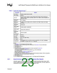
To simplify the following discussion, the processor system bus signals have been combined into
groups by buffer type. All P6 family processor system bus outputs are open drain and require a
high-level source provided termination resistors. However, the processor includes on-die
termination for AGTL signals and termination resistors placed on the platform are not necessary
except for the RESET# signal which still requires external termination.
AGTL input signals have differential input buffers which use VREF as a reference signal. AGTL
output signals require termination to 1.25 V. In this document, the term “AGTL Input” refers to the
AGTL input group as well as the AGTL I/O group when receiving. Similarly, “AGTL Output”
refers to the AGTL output group as well as the AGTL I/O group when driving.
The PWRGOOD signal input is a 1.8 V signal level and must be pulled up to VCCCMOS1.8. The
VTT_PWRGD is not 1.8 V tolerant and must be connected to VTT (1.25 V). Other CMOS inputs
(A20M#, IGNNE#, INIT#, LINT0/INTR, LINT1/NMI, PREQ#, SMI, SLP#, and STPCLK#) are
only 1.5 V tolerant and must be pulled up to VCCCMOS1.5. The CMOS, APIC, and TAP outputs are
open drain and must be pulled to the appropriate level to meet the input specifications of the
interfacing device.
The groups and the signals contained within each group are shown in Table 4. Refer to Section 7.0
for a description of these signals.
22
Datasheet

 INTEL [ INTEL ]