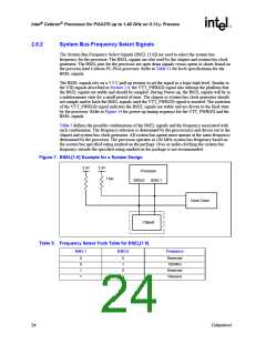
Intel® Celeron® Processor for PGA370 up to 1.40 GHz on 0.13 µ Process
on the model 68xh based on 0.18 micron process core processor. By connecting the VID25mV
signal to the Vss pin, it will disable the 25 mV stepping granularity output and the regulator will
resort to 50 mV stepping increment. The voltage regulator or VRM must supply the voltage that is
requested or disable itself.
In addition to the new signal “VID25mV”, the processor will introduce a second new signal labeled
as “VTT_PWRGD”. The VTT_PWRGD signal informs the platform that the VID and BSEL
signals are stable and should be sampled. During Power-up, the VID signals will be in an
indeterminate state for a small period of time. The voltage regulator or the VRM should not latch
the VID signals until the VTT_PWRGD signal is asserted by the VRM and sampled active. The
assertion of the VTT_PWRGD signal indicates the VID signals are stable and are driven to the
final state by the processor. Refer to Figure 14 for power-up timing sequence for the
VTT_PWRGD and the VID signals.
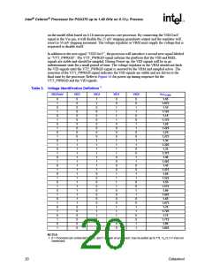
Table 3. Voltage Identification Definition 1
VID25mV
VID3
VID2
VID1
VID0
Vcc
CORE
0
1
0
1
0
1
0
1
0
1
0
1
0
1
0
1
0
1
0
1
0
1
0
1
0
1
0
1
0
1
0
1
0
0
0
0
0
0
0
0
0
0
1
1
1
1
1
1
1
1
1
1
1
1
1
1
1
1
0
0
0
0
0
0
1
1
0
0
0
0
0
0
0
0
1
1
1
1
1
1
1
1
0
0
0
0
0
0
0
0
1
1
1
1
1
1
0
0
1
1
1
1
0
0
0
0
1
1
1
1
0
0
0
0
1
1
1
1
0
0
0
0
1
1
1
1
0
0
0
0
1
1
0
0
1
1
0
0
1
1
0
0
1
1
0
0
1
1
0
0
1
1
0
0
1
1
0
0
1
1
1.05
1.075
1.10
1.125
1.15
1.175
1.20
1.225
1.25
1.275
1.30
1.325
1.35
1.375
1.40
1.425
1.45
1.475
1.50
1.525
1.55
1.575
1.60
1.625
1.65
1.675
1.70
1.725
1.75
1.775
1.80
1.825
NOTES:
1. 0 = Processor pin connected to VSS. and 1 = Open on processor; may be pulled up to TTL VIH (3.3 V max) on
baseboard.
20
Datasheet

 INTEL [ INTEL ]