Intel® Celeron® Processor for PGA370 up to 1.40 GHz on 0.13 µ Process
2.2.7
Clock Control
BCLK provides the clock signal for the processor and on-die L2 cache. During AutoHALT Power
Down and Stop-Grant states, the processor will process a system bus snoop. The processor does not
stop the clock to the L2 cache during AutoHALT Power Down or Stop-Grant states. Entrance into
the Halt/Grant Snoop state allows the L2 cache to be snooped, similar to the Normal state.
When the processor is in Sleep and Deep Sleep states, it does not respond to interrupts or snoop
transactions. During the Sleep state, the internal clock to the L2 cache is not stopped. During the
Deep Sleep state, the internal clock to the L2 cache is stopped. The internal clock to the L2 cache is
restarted only after the internal clocking mechanism for the processor is stable (i.e., the processor
has re-entered Sleep state).
PICCLK should not be removed during the AutoHALT Power Down or Stop-Grant states.
PICCLK can be removed during the Sleep or Deep Sleep states. When transitioning from the Deep
Sleep state to the Sleep state, PICCLK must be restarted with BCLK.
2.3
Power and Ground Pins
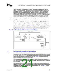
The operating voltage for the processor is the same for the core and the L2 cache. VCCCORE is
defined as the power pins that supply voltage to the processor’s core and cache. The Voltage
Regulator Module (VRM) or Voltage Regulator are controlled by the five voltage identification
(VID) signals driven by the processor. The VID signals specify the voltage required by the
processor core. Refer to Section 2.6 for further details on the VID voltage settings.
The processor has 74 VCCCORE, 7 VREF, 20 VTT, VCCCMOS1.5, VCCCMOS1.8, VCCCMOS2.0 and 74
VSS inputs. The VREF inputs are used as the AGTL reference voltage for the processor. The VTT
inputs (1.25V) are used to provide an AGTL termination voltage to the processor. VCCCMOS1.5 and
VCCCMOS1.8 and VCCCMOS2.0 are not voltage input pins to the processor but rather voltage sources
for the pullup resistors which are connected to CMOS (non-AGTL) input/output signals driven to/
from the processor. The VSS inputs are ground pins for the processor core and L2 cache.
On the platform, all VCCCORE pins must be connected to a voltage island (an island is a portion of
a power plane that has been divided, or an entire plane) to minimize any voltage drop that may
occur due to trace impedance. It is also highly recommended for the platform to provide either a
voltage island or a wide trace for the VTT pins. Similarly, all Vss pins must be connected to a
system ground plane. These recommendations can be found in the platform design guide layout
section.
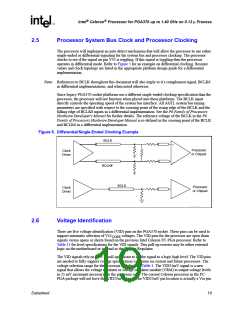
2.3.1
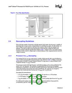
Phase Lock Loop (PLL) Power
It is highly critical that phase lock loop power delivery to the processor meets Intel’s requirements.
A low pass filter is required for power delivery to pins PLL1 and PLL2. This serves as an isolated,
decoupled power source for the internal PLL. Refer to the Phase Lock Loop Power section in the
appropriate platform design guide for the recommended filter implementation.
Datasheet
17

 INTEL [ INTEL ]