Intel® Celeron® Processor for PGA370 up to 1.40 GHz on 0.13 µ Process
2.0
Electrical Specifications
2.1
Processor System Bus and V
REF
The processor uses the original low voltage signaling of the Gunning Transceiver Logic (GTL)
technology for the system bus. The GTL system bus operates at 1.25V signal levels versus GTL+
which operates at 1.5 V signal levels. The GTL+ signal technology is used by the Intel® Pentium®
Pro, Intel® Pentium® II and Intel® Pentium® III processors.
Current P6 family processors vary from the Intel® Pentium® Pro processor in their output buffer
implementation. The buffers that drive the system bus signals on the processor are actively driven
to VTT for one clock cycle after the low to high transition to improve rise times. These signals are
open-drain and require termination to a supply. Because this specification is different from the
standard GTL specification, it is referred to as AGTL, or Assisted GTL in this and other
documentation related to the processor.
AGTL logic and AGTL+ logic are not compatible with each other due to differences with the signal
switching levels. The processor cannot be installed into platforms where the chipset only supports
the AGTL+ signal levels. For more information on AGTL or AGTL+ routing, please refer to the
appropriate platform design guide.
AGTL inputs use differential receivers which requires a reference voltage (VREF). VREF is used by
the differential receivers to determine if the input signal is a logical 0 or a logical 1. The VREF
signal is typically implemented as a voltage divider on the platform. Noise decoupling is critical for
the VREF signal. Refer to the platform design guide for the recommended decoupling requirements.
Another important item for the AGTL system bus is termination.
System bus termination is used to pull each signal to a high voltage level and to control reflections
on the transmission line. The processor contains on-die termination resistors that provide
termination for one end of the system bus. The other end of the system bus should also be
terminated near the chipset by resistors placed on the platform or on-die termination within the
chipset. It is recommended that the system bus is implemented using Dual-End Termination (DET)
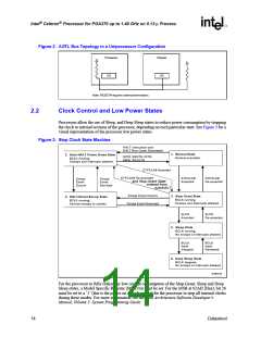
to meet the timings and signal integrity specified by the processor. Figure 2 is a schematic
representation of the AGTL bus topology for the processor, when the chipset has does not have on-
die termination.
Note: The RESET# signal requires a discrete external termination resistor on the system board.
The AGTL bus depends on incident wave switching. Therefore, timing calculations for AGTL
signals are based on flight time as opposed to capacitive deratings. Analog signal simulations of the
system bus, including trace lengths, is highly recommended especially when not following the
recommended layout guidelines.
Datasheet
13

 INTEL [ INTEL ]