INTEL StrataFlash™ MEMORY TECHNOLOGY, 32 AND 64 MBIT
E
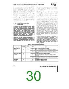
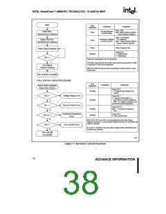
Bus
Operation
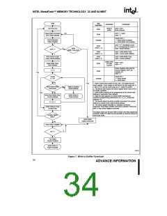
Start
Command
Comments
Set Time-Out
Write to
Buffer
Data = E8H
Block Address
Write
Read
Issue Write Command
E8H, Block Address
No
XSR. 7 = Valid
Addr = X
Check XSR. 7
Read Extended
Status Register
Standby
1 = Write Buffer Available
0 = Write Buffer Not Available
Data = N = Word/Byte Count
N = 0 Corresponds to Count = 1
Addr = Block Address
Write
(Note 1, 2)
0
Write
Buffer Time-Out?
XSR.7 =
1
Write
(Note 3, 4)
Data = Write Buffer Data
Addr = Device Start Address
Write Word or Byte
Count, Block Address
Write
(Note 5, 6)
Data = Write Buffer Data
Addr = Device Address
Buffer Write
to Flash
Confirm
Data = D0H
Addr = X
Write Buffer Data,
Start Address
Write
Read
Status Register Data with the
Device Enabled, OE# Low
Updates SR
X = 0
Yes
Addr = X
Check SR.7
1 = WSM Ready
0 = WSM Busy
Check
X = N?
Standby
No
Yes
1. Byte or word count values on DQ0-DQ 7 are loaded into the
count register. Count ranges on this device for byte mode are
= 00H to 1FH and for word mode are N = 0000H to 000FH.
2. The device now outputs the status register when read (XSR is
no longer available).
N
Abort Buffer Write
Command?
Yes
Write to Another
Block Address
3. Write Buffer contents will be programmed at the device start
address or destination flash address.
4. Align the start address on a Write Buffer boundary for
maximum programming performance (i.e., A4- A 0 of the start
address = 0).
Yes
No
Write Next Buffer Data,
Device Address
Buffer Write to
Flash Aborted
5. The device aborts the Write to Buffer command if the current
address is outside of the original block address.
6. The status register indicates an "improper command
sequence" if the Write to Buffer command is aborted. Follow this
with a Clear Status Register command.
X = X + 1
Buffer Write to Flash
Confirm D0H
Full status check can be done after all erase and write sequences
complete. Write FFH after the last operation to reset the device to
read array mode.
Another Buffer
Write?
Issue Read
Status Command
No
Read Status Register
0
SR.7 =
1
Full Status
Check if Desired
Buffer Write to
Flash Complete
0606_07
Figure 7. Write to Buffer Flowchart
34
ADVANCE INFORMATION

 INTEL [ INTEL ]