E
INTEL StrataFlash™ MEMORY TECHNOLOGY, 32 AND 64 MBIT
4.2.3
BLOCK STATUS REGISTER
The Block Status Register indicates whether a given block is locked and can be accessed for program/erase
operations. On SCS devices that do not implement block locking, BSR.0 will indicate functional block status
on partially functional devices. The Block Status Register is accessed from word address 02h within each
block.
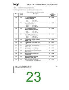
Table 8. Block Status Register
Offset
Length
(bytes)
Description
Intel StrataFlash™
Memory
x16 device/mode
(BA +2)h1
01h
Block Status Register
BSR.0 = Block Lock or Non-Functional Status
BA+2: 0000h or
0001h
BA+2 (bit 0): 0 or 1
(Optional)
1 = Locked or Non-Functional
0 = Unlocked
BSR.1 = Block Erase or Non-Functional
Status(2) (Optional)
BA+2 (bit 1): 0
(The device does
not support Block
Erase Status)
1 = Last erase operation did
not complete successfully or Non-
Functional
0 = Last erase operation
completed successfully or Functional
BSR 2–7 Reserved for future use
BA+2 (bits 2–7): 0
NOTES:
1. BA = The beginning location of a Block Address (i.e., 2000h is the beginning location of block 2).
2. Block Erase Status is an optional part of the SCS definition and is not incorporated on this device.
21
ADVANCE INFORMATION

 INTEL [ INTEL ]