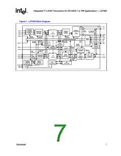
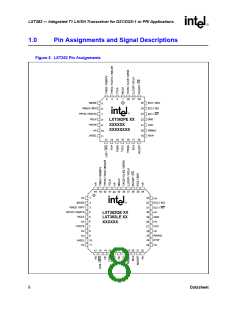
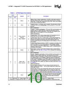
LXT362 — Integrated T1 LH/SH Transceiver for DS1/DSX-1 or PRI Applications
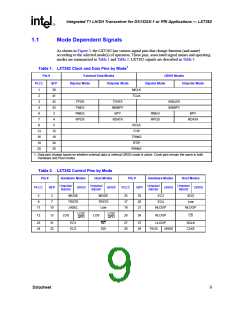
Table 3. LXT362 Signal Descriptions
Pin #
Symbol
I/O1
Description
PLCC
QFP
Master Clock. External, independent 1.544 MHz clock signal required to
generate internal clocks. MCLK must be jitter-free and have an accuracy
better than ± 50 ppm with a typical duty cycle of 50%. Upon Loss of Signal
(LOS), RCLK is derived from MCLK.
1
39
MCLK
TCLK
DI
DI
Transmit Clock. A 1.544 MHz clock is required. The transceiver samples
TPOS and TNEG on the falling edge of TCLK (or MCLK, if TCLK is not
present).
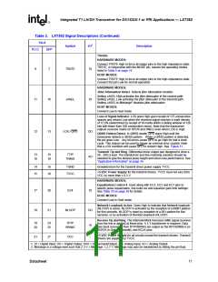
2
41
BIPOLAR MODES:
Transmit – Positive and Negative. TPOS and TNEG are the positive and
negative sides of a bipolar input pair. Data to be transmitted onto the
twisted-pair line is input at these pins. TPOS/TNEG are sampled on the
falling edge of TCLK (or MCLK, if TCLK is not present).
UNIPOLAR MODES:
Transmit Data. TDATA carries unipolar data to be transmitted onto the
3
4
42
43
DI
DI
twisted-pair line and is sampled on the falling edge of TCLK.
TPOS / TDATA /
INSLER
Transmit Insert Logic Error. In QRSS mode, a Low-to-High transition on
INSLER inserts a logic error into the transmitted QRSS data pattern. The
inserted error follows the data flow of the active loopback mode. The
LXT362 samples this pin on the falling edge of TCLK (or MCLK, if TCLK is
not present).
TNEG / INSBPV
Transmit Insert Bipolar Violation. INSBPV is sampled on the falling edge
of TCLK (or MCLK, if TCLK is not present) to control Bipolar Violation
(BPV) insertions in the transmit data stream. A Low-to-High transition is
required to insert each BPV. In QRSS mode, the BPV is inserted into the
transmitted QRSS pattern.
Mode Select. Connect Low to select Hardware mode. Connect High to
select Host mode. See Table 5 on page 19 for a complete list of operating
modes.
5
2
MODE
DI
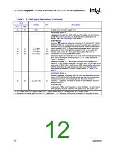
BIPOLAR MODES:
Receive – Negative and Positive. RPOS and RNEG are the positive and
negative sides of a bipolar output pair. Data recovered from the line
interface is output on these pins. A signal on RNEG corresponds to receipt
of a negative pulse on RTIP/RRING. A signal on RPOS corresponds to
receipt of a positive pulse on RTIP/RRING. RNEG/RPOS are Non-Return-
to-Zero (NRZ). In Hardware mode, RPOS/RNEG are stable and valid on
the rising edge of RCLK. In Host mode, the CLKE pin selects the RCLK
clock edge when RPOS /RNEG are stable and valid as described in Table
4 on page 18.
6
7
3
4
RNEG / BPV
DO
DO
RPOS / RDATA
UNIPOLAR MODES:
Receive Bipolar Violation. BPV goes High to indicate detection of a
bipolar violation from the line. This is an NRZ output and is valid on the
rising edge of RCLK.
Receive Data. RDATA is the unipolar NRZ output of data recovered from
the line interface. In Hardware mode, RDATA is stable and valid on the
rising edge of RCLK. In Host mode, the CLKE pin selects the RCLK clock
edge when RDATA is stable and valid as described in Table 4 on page 18.
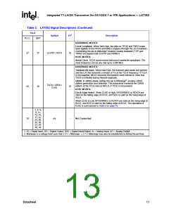
Receive Recovered Clock. The clock recovered from the line input signal
is output on this pin. Under LOS conditions, there is a smooth transition
from the RCLK signal (derived from the recovered data) to the MCLK
signal, which appears at the RCLK pin.
8
5
RCLK
DO
1. DI = Digital Input; DO = Digital Output; DI/O = Digital Input/Output; AI = Analog Input; AO = Analog Output.
2. Midrange is a voltage level such that 2.3 V ≤ Midrange ≤ 2.7 V. Midrange may also be established by letting the pin float.
10
Datasheet

 INTEL [ INTEL ]